Official websites use .gov
A .gov website belongs to an official government organization in the United States.
Secure .gov websites use HTTPS
A lock (
) or https:// means you’ve safely connected to the .gov website. Share sensitive information only on official, secure websites.
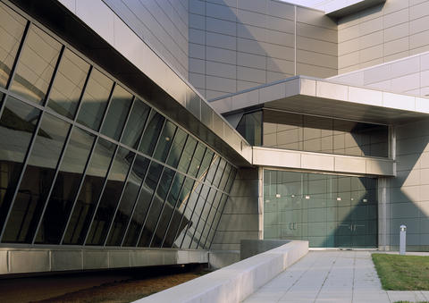
Entrance to NIST's Advanced Measurement Laboratory in Gaithersburg, Maryland.
Roche Sequencing Solutions engineer Juraj Topolancik was looking for a way to decode DNA from cancer patients in a matter of minutes.
Rajesh Krishnamurthy, a researcher with the startup company 3i Diagnostics, needed help in fabricating a key component of a device that rapidly identifies infection-causing bacteria.
Ranbir Singh, an engineer with GeneSiC Semiconductor Inc., in Dulles, Virginia, sought to construct and analyze a semiconductor chip that transmits voltages large enough to power electric cars and spacecraft.
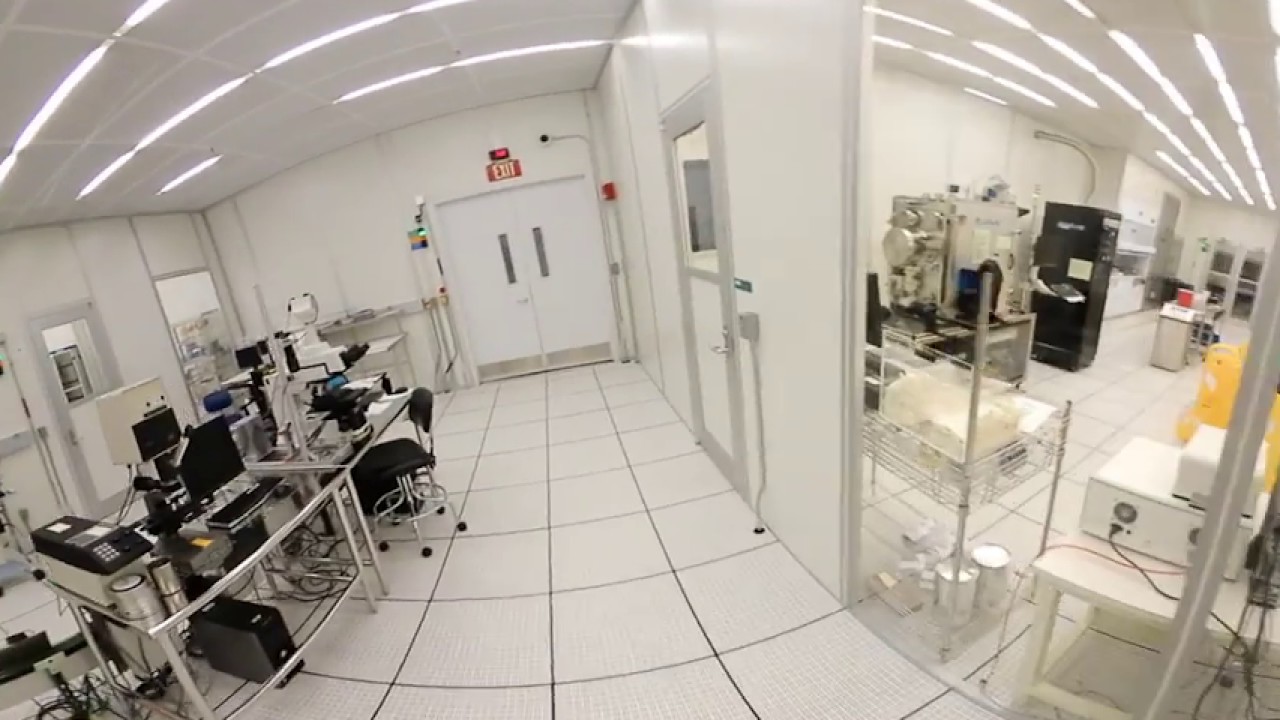
These researchers all credit the NanoFab, located at the Center for Nanoscale Science and Technology (CNST) on the Gaithersburg, Maryland campus of the National Institute of Standards and Technology (NIST). The NanoFab provides cutting-edge nanotechnology capabilities for NIST scientists that is also accessible to outside users, with supplying the state-of-art tools, know-how and dependability to realize their goals.
When Krishnamurthy, whose company is based in Germantown, Maryland, needed an infrared filter for the bacteria-identifying chip, proximity was but one factor in reaching out to the NanoFab.
“Even more important was the level of expertise you have here,” he says. “The attention to detail and the trust we have in the staff is so important—we didn’t have to worry if they would do a good job, which gives us tremendous peace of mind,” Krishnamurthy notes.
The NanoFab also aided his project in another, unexpected way. Krishnamurthy had initially thought that the design for his company’s device would require a costly, highly customized silicon chip. But in reviewing design plans with engineers at the NanoFab, “they came up with a very creative way” to use a more standard, less expensive silicon wafer that would achieve the same goals, he notes.
“The impact in the short term is that we didn’t have to pay as much [to build and test] the device at the NanoFab, which matters quite a bit because we’re a start-up company,” says Krishnamurthy. “In the long run, this will be a huge factor in [enabling us to mass produce] the device, keeping our costs low because, thanks to the input from the NanoFab, the source material is not a custom material.”
Singh came to the NanoFab with a different mission. His company is developing a gallium nitride semiconductor device durable enough to transmit hundreds to thousands of volts without deteriorating. He relies on the NanoFab’s metal deposition tools and high-resolution lithography instruments to finish building and assess the properties of the device.

“Not only is there a wide diversity of tools, but within each task there are multiple technologies,” Singh adds.
For instance, he notes, technologies offered at the NanoFab for depositing exquisitely thin and highly uniform layers of metal—which Singh found crucial for making reliable electrical contacts—include both evaporation and sputtering, he says.
The wide range of metals available for deposition at the NanoFab, uncommon at other nanotech facilities, was another draw.
“We needed different metals compared to those commonly used on silicon wafers and the NanoFab provided those materials,” notes Singh.
Topolancik, the Roche Sequencing Solutions engineer, needed high precision etching and deposition tools to fabricate a device that may ultimately improve cancer treatment. His company‘s plan to rapidly sequence DNA from cancer patients could quickly determine if potential anti-cancer drugs and those already in use are producing the genetic mutations necessary to fight cancer.
“We want to know if the drug is working, and if not, to stop using it and change the treatment,” says Topolancik.
In the standard method to sequence the double-stranded DNA molecule, a strand is peeled off and resynthesized, base by base, with each base—cytosine, adenine, guanine and thymine—tagged with a different fluorescent label.
“It’s a very accurate but slow method,” says Topolancik.
Instead of peeling apart the molecule, Topolancik is devising a method to read DNA directly, a much faster process. Borrowing a technique from the magnetic recording industry, he sandwiches the DNA between two electrodes separated by a gap just nanometers in width.

According to quantum theory, if the gap is small enough, electrons will spontaneously “tunnel” from one electrode to the other. In Topolancik’s setup, the tunneling electrons must pass through the DNA in order to reach the other electrode.
The strength of the tunneling current identifies the bases of the DNA trapped between the electrodes. It’s an extremely rapid process, but for the technique to work reliably, the electrodes and the gap between them must be fabricated with extraordinarily high precision.
That’s where the NanoFab comes in. To deposit layers of different metals just nanometers in thickness on a wafer, Topolancik relies on the NanoFab’s ion beam deposition tool. And to etch a pattern in those ultrathin, supersmooth layers without disturbing them—a final step in fabricating the electrodes—requires the NanoFab’s ion etching instrument.
“These are specialty tools that are not usually accessible in academic facilities, but here [at the NanoFab] you have full, 24/7 access to them,” says Topolancik. “And if a tool goes down, it gets fixed right away,” he adds. “People here care about you, they want you to succeed because that’s the mission of the NanoFab.” As a result, he notes, “I can get done here in two weeks what would take half a year any place else.”