
Official websites use .gov
A .gov website belongs to an official government organization in the United States.
Secure .gov websites use HTTPS
A lock (
) or https:// means you’ve safely connected to the .gov website. Share sensitive information only on official, secure websites.
Engineers at the NIST Center for Nanoscale Science and Technology (CNST) have developed a new technique for fabricating high aspect ratio three-dimensional (3D) nanostructures over large device areas using a combination of electron beam (e-beam) lithography, photolithography, and resist spray coating. While it has long been possible to make complicated 3D structures with many mask layers or expensive grayscale masks, the new technique enables researchers to etch trenches and other high aspect ratio structures with nanometer scale features without using masks and in only two process stages.
The fabrication of 3D semiconductor and dielectric structures that are patterned by exposing resist with varying intensity grayscale gradients has been essential to a broad range of applications such as digital lenses, micro-electromechanical systems, and fluidic medical devices.
Unlike devices that rely on conventional masks, which have areas that simply transmit or block light to form a pattern, the fabrication of these devices has typically relied on 3D grayscale masks which have varying levels of transparency and depend on the use of proprietary materials. Because the chemistry is proprietary and because the masks are prepared using complicated processes best suited to small surface areas, they are often prohibitively expensive. The next generation of these devices requires lower costs, larger surface areas, and ever-smaller feature sizes.
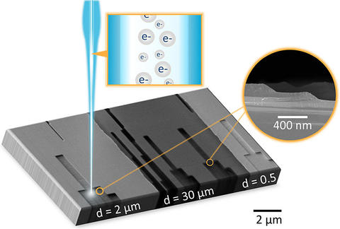
The researchers' new approach capitalizes on the high throughput capability of photolithography to generate large area grayscale structures with large processing flexibility and the ability of e-beam lithography to add grayscale features smaller than 200 nm. The first phase of this mix-and-match approach is to pattern a layer of photoresist by exposing it with a focused laser beam. By locally modulating the intensity of the light to form a grayscale gradient, varying levels of photoreaction in the photoresist are generated. After the sample is immersed in the developer solution, material is dissolved in areas corresponding to the degree of induced photoreaction, leaving the photoresist layer with varying thicknesses matching the initial exposure pattern. The sample is exposed to a deep reactive ion etch (DRIE) which removes substrate material at varying depths that depend on the thickness of the photoresist, transferring the 3D photoresist pattern vertically into the substrate to form deep grayscale micro-structures. The second phase applies similar processing steps but with feature sizes ten times smaller. First, a high pressure e-beam resist spray coating is applied to obtain conformal coverage of the high-aspect ratio topography produced in the first phase. Then, by manipulating a high-energy e-beam with nanometer-scale resolution, patterned grayscale step heights are directly written in the e-beam resist in different locations. Finally, the resist is developed and the sample is exposed to DRIE as it was in the first step.
The two stage process results in a vertical feature sizes of 45 ± 6 nm within a substrate structure that varies from 2 μm to 30 μm deep and with horizontal feature sizes of 100 nm to 200 nm and an overall pattern size potentially as large as a whole wafer. CNST NanoFab Process Engineer Liya Yu anticipates that the ability to fabricate high aspect-ratio grayscale nanostructures will expand the practical applications of grayscale lithography and dramatically widen the range of device structures available to device designers.
*The evaluation of photo/e-beam complementary grayscale lithography for high topography 3D structure, L. Yu, R. J. Kasica, R. N. Newby, L. Chen, and V. K. Luciani, Proceedings of SPIE 8682, 868212 (2013).
NIST Publication Database Journal Web Site