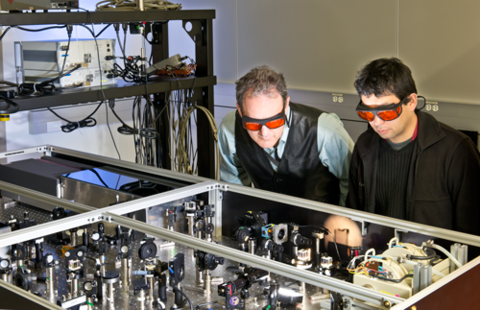
Tom Silva (left) and Hans Nembach examine the partially disassembled original H-MOMM set-up. The entire configuration is being re-built to measure damping on smaller structures and different magnetic field orientations.
If spintronics is to become the Next Big Thing, it will be because researchers have learned how to control many extremely small, but hugely significant, things. Now PML scientists have devised a unique method of measuring one of the most important of those: the "damping" properties of individual magnetic nanostructures, or nanomagnets, that store and transfer information for random-access memory and other uses.
"This is new metrology," says Ron Goldfarb, leader of the Magnetics Group in PML's Electromagnetics Division. "These are new measurement techniques that nobody conceived of before. They are vitally necessary so that the people who are making these spintronic devices can know whether they are going to work or not, and how to adjust their manufacturing processes accordingly."
Whereas conventional transistors depend on fast and reliable switching of electronic signals, spintronic devices manipulate the spin states of electrons instead of current or voltage. Thus they require much less power and can operate much faster than electronic systems. Their performance is determined by the ability of magnetic nanostructures tens to hundreds of nanometers wide to switch spin states quickly and consistently, and to remain in the altered state for the right amount of time.
Spin switching, in turn, is critically dependent on damping, the degree to which the nanostructure resists switching spins or relaxing back to its pre-excitation condition. If the damping is too great, the structure will require too much power to switch. (Reducing the current needed by a factor of two reduces the unit's power consumption by a factor of four.) So ideally, the damping parameter should be as low as possible.

"The notion that spintronics is going to replace conventional DRAM is based on the assumption that this is a highly scalable technology," says Tom Silva, who heads the project team that recently published the breakthrough measurements in Physical Review Letters. "According to the physics that most people think is operative, damping should not scale with size. That is, it should be the same whether you're talking about a 10 nm structure or a 1000 nm structure. But that had never been convincingly demonstrated.
"For us, the big questions were: Is there unknown physics of the magnetic materials as you go into these extremely small dimensions, and is the presumption that you can scale correct?"
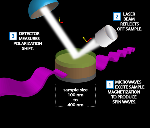
To measure damping in individual nanomagnets on the order of 100 nm in diameter, Silva and colleagues had to invent an instrument called the H-MOMM: the heterodyne magneto-optical microwave microscope. Built by project team member Hans Nembach, it took five years to develop and eventually comprised more than 100 components on an optical table.
The group used the one-of-a-kind apparatus to examine elliptical nanomagnet samples made by project team member Justin Shaw in three sizes (440 x 400 nm, 240 x 200 nm, and 120 x 100 nm), each containing a single layer of nickel-iron alloy. To excite the sample, the researchers combined two laser beams to generate beat-frequency microwaves that were conveyed to the sample via a waveguide. The microwaves produced propagating oscillations of magnetic disturbance called spin waves which acted on the sample nanomagnet's spin state.

The signal from a single nanostructure is exceedingly faint, so after the reflected light passed through a polarization analyzer, the MOKE beam was used to modulate a much brighter laser beam, dramatically improving the signal-to-noise ratio.
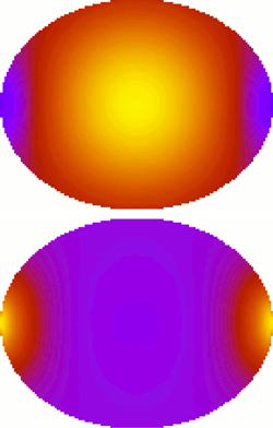
By applying microwaves over a frequency range of 4 GHz to 17 GHz, the researchers observed that magnetic oscillations in the nanomagnets had two predominant modes: a "center" mode and an "end" mode, each of which had different damping characteristics depending on the nanomagnet size. [See diagram at right.]
For larger nanomagnet sizes, the end modes were more strongly damped than the center mode. In the 100 nm nanomagnets, the reverse was true. In addition, damping seemed to increase as the wavelength of the spin waves got shorter. In all, the results were convincing evidence that uniform scaling does not occur.
In all cases, individual nanomagnets showed larger damping than the bulk film, and the degree of damping depended on the size and spin-wave mode. "What we found," Silva says, "is that the more uniform the excitation – that is, the more the spins are all moving at the same amplitude in lock step – the smaller the damping. If you have some of these end modes, even though they're all at the same frequency, it drives the dissipation."

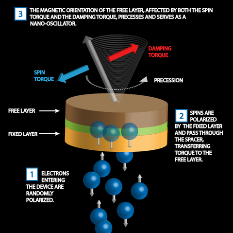
As those polarized electrons arrive, they transfer their spin to the free layer. That layer's magnetic orientation begins to precess in response to two competing torques – the spin torque from the polarized electrons and the natural damping tendency of the material.
"There are several practical uses," Goldfarb says. "For example, in any system you have to get signals from one component to another. In conventional chips, this is done by traces, and you get losses in the transfer. But what if you had wireless transmission, with the oscillator on one chip and the receiver on the other? This would be a very energy-efficient, and very fast, way to exchange information."
Those and other phenomena will be investigated with the new, second-generation H-MOMM now under construction. The original has been disassembled and will be enhanced with a 3 T field magnet and the ability to address individual nanomagnets below 50 nm in size, among other improvements.
"Our work is at this sort of dirty knife edge between fundamental physics and relevance to industry," Silva says. "Spintronics is really in a sweet spot for applications. But in the devices themselves, we don't yet know what all the important independent variables are. It's a whole new field."

