
Official websites use .gov
A .gov website belongs to an official government organization in the United States.
Secure .gov websites use HTTPS
A lock (
) or https:// means you’ve safely connected to the .gov website. Share sensitive information only on official, secure websites.
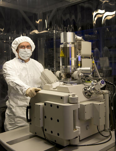
Dr. András Vladár operates the NIST dimensional metrology reference SEM.
Since the inception of the scanning electron microscope (SEM), users have encountered the persistent problem of contamination. Cleanliness is required for imaging and to make good quality measurements, and PML has led the exploration and the development of methods to allow SEM users gather high-quality, repeatable, and quantitative measurement results.
Developing the cleaning procedures and devices necessary for the process took years of research and collaboration with industry. But today it is possible to make contamination in the SEM a thing of the past. Users can now measure the exact features of the sample, not the sample features plus a layer of contamination. This is especially important for the integrated circuit industry where it is estimated that a 1 nm improvement in integrated circuit technology leads to an estimated 1 billion dollars or more in extra economic value produced.1
Although many contamination problems have been addressed, research continues at PML, where scientists, led by András Vladár of the Semiconductor and Dimensional Metrology Division (SDMD), are examining promising improvements to the existing SEM and sample cleaning methods.
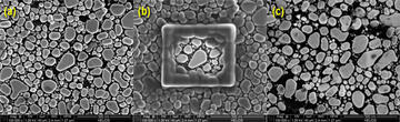
Charged particle beam-induced contamination in SEMs manifests itself as a gradual buildup of carbonaceous material on the surface of the sample where the ions or electrons are focused, resulting in characteristic dark patterns. Such contamination, typically caused by residual organic materials in the SEM apparatus itself, changes the sample, as well as the number, trajectory, and energy of the electrons leaving the sample, making repeatable quantitative measurements difficult or impossible.
As a result, contamination has become a showstopper for measurements at the nanometer scale, which require a level of cleanliness far beyond what was acceptable in the past.
"If contamination is present," Vladár states, "sometimes you simply cannot do the work. And, even if the contamination does not prevent the work, it changes the amount and the energy of the electrons, so misleading measurement results can occur.
The battle against SEM contamination began in the 1990s prior to Vladár joining NIST, led originally by the SDMD's Michael Postek. In a collaborative effort with a small U.S. company, they tested and confirmed the usefulness of a prototype low-energy (20 W) plasma unit that was designed by XEI Scientific to hook into an SEM access port and clean the instrument by flooding it with oxygen plasma.
Research with this cleaning unit continued after Vladár joined NIST's SEM project in 1999. The project conducted tests on such variables as the optimal plasma pressure range and how much cleaning time is actually needed for the best results. The project's scientists reached the realization that it's not enough to simply have a clean instrument—a clean reference sample is also indispensable.
"Even with a clean instrument, you can have a contamination problem if the sample itself is dirty," Vladár explains. "We needed to develop a good sample cleaning procedure to obtain a reference sample. You need to be able to use a known-clean sample to allow you to make the distinction between instrument dirt and sample dirt."
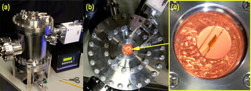
Another collaboration with IBSS Group led to a modified plasma-cleaning device that works in a wider vacuum range and also has higher power, up to 99 watts. While low power is sufficient for oxygen-based plasma cleaning, oxygen-sensitive samples (for example evaporated gold on carbon resolution samples, which can be damaged by oxygen gas) need hydrogen or helium plasma cleaning, where higher power is very helpful.
The decades of effort by Vladár, Postek, and others have led to a NIST Contamination Specification, steps that SEM users worldwide can take to determine whether their instruments need to be cleaned and how to implement an effective cleaning process.2 Today there are more than 2,300 low-energy plasma-cleaning devices in use.
"We know how to get the instruments clean, and we know how to clean the samples." Vladár states. "We learned that when you clean it, the instrument can remain contamination free for months unless a dirty sample is used. Our efforts show that government researchers teamed up with small U.S. companies can help to solve serious problems in research and industry."
New research at PML indicates that the electron bombardment itself during extended measurements can act as a cleaning process for a variety of samples. Vladár hypothesizes that, because any surface that has been exposed to air will collect a very thin layer of water on the surface, it is possible that this layer is being removed during the electron bombardment. This new finding has the potential to help SEM users reach a level of ultimate cleanliness that could possibly eliminate the necessity for the use of an ultra-high vacuum, which could help make measurements easier and cheaper.
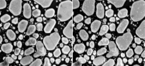
The center magnified portions of the above hydrogen-cleaned evaporated gold-on-carbon sample after hydrogen plasma cleaning. Area imaged initially (left) and after 10 minutes of continuous imaging at twice as high magnification (right). Clearly better resolution with more sample details can be realized after both hydrogen plasma and electron cleaning was applied.
Additional research at PML will be focused on determining exactly how and why the cleaning process works. "We are trying to analyze the surfaces to find out exactly what is happening," Vladár explains.
Outside of his lab, the NIST efforts on the cleaning techniques continue to be felt with the incorporation of this proven process into other tools such as transmission electron microscopes and extreme ultraviolet imagers.
"When you have a method that works," he concludes, "you start to apply it to different fields."
1C. P. Ausschnitt and M. E. Lagus, "Seeing the Forest for the Trees: A New Approach to CD control," Proc. SPIE Vol. 3332, p. 212 (1998) and J. S. Villarrubia, A. E. Vladar and M. T. Postek, Scanning electron microscope dimensional metrology using a model-based library, Surf. Interface Anal. (2005)
2A. E. Vladár, K. P. Purushotham and M. T. Postek, "Contamination Specification for Dimensional Metrology SEMs," Proc. SPIE Vol. 6922 (2008)