
Official websites use .gov
A .gov website belongs to an official government organization in the United States.
Secure .gov websites use HTTPS
A lock (
) or https:// means you’ve safely connected to the .gov website. Share sensitive information only on official, secure websites.
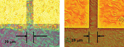
Optical micrographs of typical FET structures in the NIST/Penn State/UK experiments show the effect of pretreating contacts to promote organic crystal formation. Treated structure (l) shows crystal structure extending from the rectangular contacts and merging in the channel in contrast to untreated contacts (r).
A simple surface treatment technique demonstrated by a collaboration between researchers at the National Institute of Standards and Technology (NIST), Penn State and the University of Kentucky potentially offers a low-cost way to mass produce large arrays of organic electronic transistors on polymer sheets for a wide range of applications including flexible displays, "intelligent paper" and flexible sheets of biosensor arrays for field diagnostics.
In a paper posted this week, the team describes how a chemical pretreatment of electrical contacts can induce self-assembly of molecular crystals to both improve the performance of organic semiconductor devices and provide electrical isolation between devices.
Organic electronic devices are inching towards the market. Compounds with tongue-twisting names like "5,11-bis(triethylsilylethynyl) anthradithiophene" can be designed with many of the electrical properties of more conventional semiconductors. But unlike traditional semiconductors that require high-temperature processing steps, organic semiconductor devices can be manufactured at room temperature. They could be built on flexible polymers instead of rigid silicon wafers. Magazine-size displays that could be rolled up or folded to pocket size and plastic sheets that incorporate large arrays of detectors for medical monitoring or diagnostics in the field are just a couple of the tantalizing possibilities.
One unsolved problem is how to manufacture them efficiently and at low cost. Large areas can be coated rapidly with a thin film of the organic compound in solution, which dries to a semiconductor layer. But for big arrays like displays, that layer must be patterned into electrically isolated devices. Doing that requires one or more additional steps that are costly, time-consuming and/or difficult to do accurately.
The NIST team and their partners studied the organic version of a workhorse device—the field effect transistor (FET)—that commonly is used as a switch to, for example, turn pixels on and off in computer displays. The essential structure consists of two electrical contacts with a channel of semiconductor between them. The researchers found that by applying a specially tailored pretreatment compound to the contacts before applying the organic semiconductor solution, they could induce the molecules in solution to self-assemble into well-ordered crystals at the contact sites. These structures grow outwards to join across the FET channel in a way that provides good electrical properties at the FET site, but further away from the treated contacts the molecules dry in a more random, helter-skelter arrangement that has dramatically poorer properties—effectively providing the needed electrical isolation for each device without any additional processing steps. The work is an example of the merging of device structure and function that may enable low cost manufacturing, and an area where organic materials have important advantages.
In addition to its potential as a commercially important manufacturing process, the authors note, this chemically engineered self-ordering of organic semiconductor molecules can be used to create test structures for fundamental studies of charge transport and other important properties of a range of organic electronic systems.
Paper: D.J. Gundlach, J.E. Royer, S.K. Park, S. Subramanian, O.D. Jurchescu, B.H. Hamadani, A.J. Moad, R.J. Kline, L.C. Teague, O. Kirillov, C.A. Richter, J.G. Kushmerick, L.J. Richter, S.R. Parkin, T.N. Jackson and J.E. Anthony. Contact-induced crystallinity for high-performance soluble acene-based transistors and circuits. Nature Materials Advanced Online Publication, 17 February 2008.