
Official websites use .gov
A .gov website belongs to an official government organization in the United States.
Secure .gov websites use HTTPS
A lock (
) or https:// means you’ve safely connected to the .gov website. Share sensitive information only on official, secure websites.
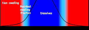
Schematic of the photolithography process shows the formation of a gradient extending from the photoresist material to be removed (center) into the unexposed portions of the resist on the sides. NIST measurements document the residual swelling fraction caused by the developer that can contribute to roughness in the final developed image.
Scientists at the National Institute of Standards and Technology (NIST) have made the first direct measurements of the infinitesimal expansion and collapse of thin polymer films used in the manufacture of advanced semiconductor devices. It's a matter of only a couple of nanometers, but it can be enough to affect the performance of next-generation chip manufacturing. The NIST measurements, detailed in a new paper, offer a new insight into the complex chemistry that enables the mass production of powerful new integrated circuits.
The smallest critical features in memory or processor chips include transistor "gates." In today's most advanced chips, gate length is about 45 nanometers, and the industry is aiming for 32-nanometer gates. To build the nearly one billion transistors in modern microprocessors, manufacturers use photolithography, the high-tech, nanoscale version of printing technology. The semiconductor wafer is coated with a thin film of photoresist, a polymer-based formulation, and exposed with a desired pattern using masks and short wavelength light (193 nm). The light changes the solubility of the exposed portions of the resist, and a developer fluid is used to wash the resist away, leaving the pattern which is used for further processing.
Exactly what happens at the interface between the exposed and unexposed photoresist has become an important issue for the design of 32-nanometer processes. Most of the exposed areas of the photoresist swell slightly and dissolve away when washed with the developer. However this swelling can induce the polymer formulation to separate (like oil and water) and alter the unexposed portions of the resist at the edges of the pattern, roughening the edge. For a 32-nanometer feature, manufacturers want to hold this roughness to at most about two or three nanometers.
Industry models of the process have assumed a fairly simple relationship in which edge roughness in the exposed "latent" image in the photoresist transfers directly to the developed pattern, but the NIST measurements reveal a much more complicated process. By substituting deuterium-based heavy water in the chemistry, the NIST team was able to use neutrons to observe the entire process at a nanometer scale. They found that at the edges of exposed areas the photoresist components interact to allow the developer to penetrate several nanometers into the unexposed resist. This interface region swells up and remains swollen during the rinsing process, collapsing when the surface is dried. The magnitude of the swelling is significantly larger than the molecules in the resist, and the end effect can limit the ability of the photoresist to achieve the needed edge resolution. On the plus side, say the researchers, their measurements give new insight into how the resist chemistry could be modified to control the swelling to optimal levels.
The research, funded by SEMATECH, is part of a NIST-industry effort to better understand the complex chemistry of photoresists in order to meet the needs of next-generation photolithography.
V.M. Prabhu, B.D. Vogt, S. Kang , A. Rao , E.K. Lin and S.K. Satija. Direct measurement of the spatial extent of the in situ developed latent image by neutron reflectivity. Journal of Vacuum Science and Technology B, 25(6), 2514-2520 (2007).