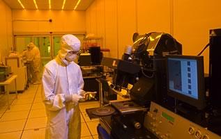
CNST and its Nanofabrication Facility are housed in NIST's new Advanced Measurement Laboratory, one of the most advanced research facilities in the world.
University, industry, government and other researchers who need access to state-of-the-art and beyond-state-of-the-art facilities to study a wide range of nanotechnology topics now have a new resource. The Commerce Department's National Institute of Standards and Technology (NIST) announced today that its Center for Nanoscale Science and Technology (CNST) is now accepting proposals for nanotechnology-related research projects. Established in March 2006, the new center focuses on overcoming major technical obstacles to cost-effective manufacturing of products made with components the size of atoms and molecules. In particular, the center's mission is to support innovation in the field by developing measurement methods, standards and technology that help emerging nanotechnologies move from the laboratory to production. The center is located within NIST's Advanced Measurement Laboratory, one of the most advanced research facilities of its kind in the world.
"Researchers from industry, academia or government, whose own work is limited by their inability to make or measure nanoscale devices will benefit the most," said CNST Director Robert Celotta. "We've specifically staffed and equipped the CNST to help solve the problems that are slowing the movement of nanotechnology from discovery to market."
NIST's CNST consists of both an active interdisciplinary research program and a national user facility, a 16,000 square foot [1486 square meters] nanofabrication facility. About half of the nanofabrication facility is devoted to class 100 cleanroom space. The nanofabrication facility includes more than 30 state-of-the-art tools such as photolithography, ion beam and etching equipment capable of creating, measuring and inspecting nanoscale devices with dimensions as small as 10 nanometers (billionths of a meter).
The center is supported by a current NIST staff of 40 that is expected to grow in the coming year, according to Celotta. Current NIST research areas include: devices, architectures and interconnects for next-generation electronics; top-down and bottom-up fabrication and assembly for nanomanufacturing and nanofabrication; and conversion, storage and transport research with energy applications.

In addition, Celotta noted that the center has a five-year $7.5 million cooperative agreement in place with the University of Maryland NanoCenter. The agreement calls for about 10 to 12 University of Maryland scientists and engineers to participate with CNST researchers on collaborative projects at any one time, and it provides support for training programs, nanotechnology workshops, professional development and outreach efforts to the broader nanotechnology research community.
"We are pleased to support the efforts of the center. Our partnership with NIST is central to our extensive research efforts in nanotechnology. The special opportunity provided through the partnership of a national laboratory and a university allows us both to do work we could not otherwise do. This is an exciting time and we expect great achievements," said University of Maryland President C.D. Mote, Jr.
Researchers interested in working at the facility can now submit proposals for review in any nanotechnology research area. According to the center's Web site, the center will accept both proprietary and non-proprietary research proposals. Non-proprietary research may qualify for a partial waiver of use fees if the project falls within CNST's mission. Non-proprietary proposals are expected to lead to publication of research results in the open scientific literature.
Detailed information about the proposal process, available facilities, current CNST research programs and contact information for fee schedules is available online.

