
Official websites use .gov
A .gov website belongs to an official government organization in the United States.
Secure .gov websites use HTTPS
A lock (
) or https:// means you’ve safely connected to the .gov website. Share sensitive information only on official, secure websites.
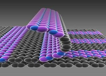
2D layered materials are like color papers: they can be glued, stacked, cut and folded to form integrated devices with atomic thickness. In this talk, I will discuss how different 2D materials can be grown with distinct electrical and optical properties (coloring), how they can be connected laterally to form pattered circuits (stitching) and how their interaction with light can be designed by controlling the interlayer rotation and the valley degree of freedom (twisting).
For further information please contact robert.ilic [at] nist.gov (Robert Ilic), 301-975-2639.
Speakers
Jiwoong Park
Chemistry and Molecular Engineering
University of Chicago