
Official websites use .gov
A .gov website belongs to an official government organization in the United States.
Secure .gov websites use HTTPS
A lock (
) or https:// means you’ve safely connected to the .gov website. Share sensitive information only on official, secure websites.
Positron Annihilation Lifetime Spectrometer
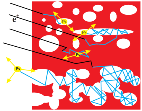
Positronium formation inside polymer materials [1].
Positron annihilation lifetime spectroscopy uses positrons to probe material defects/voids/free volume at the sub-nm scale. The general working principle is based on correlating the lifetime (dwelling time) of the injected positrons against the sample void size (longer lifetimes correspond to large void sizes). The table-top spectrometer has a time resolution of ~ 270 ps, and uses a 22Na positron source sandwiched between two thin Kapton foils. The source is sandwiched between the material of interest and the annihilation lifetimes and intensities are deconvoluted by fitting exponential decay functions using commercially available software. Here, the spectrometer is primarily used to understand polymeric materials and fiber reinforced composites. Thermalized positrons form a quasi-bound state with electrons, known as positronium (Ps) that localize within void-content of polymers. The Ps eventually pick-off an electron from neighboring atoms to annihilate within 1-10 ns which can then be correlated against the free volume nanohole radius using a semi-empirical Tao-Eldrup equation.
Reference:
[1] Gidley DW, Peng H-G, Vallery RS. Positron Annihilation As a Method To Characterize Porous Materials. Annu Rev Mater Res 2006;36:49–79. doi:10.1146/annurev.matsci.36.111904.135144.
Specifications/Capabilities/Limitations
-
Capable of resolving voids in polymers, metals and semiconductors having a size range of less than a nm.
-
Weak positron source, slow acquisition rate: typical measurement times approximately 5 days to 10 days per set of sample:
-
-
Metals and Semiconductors: 2 samples, ~ 0.5 mm in thickness.
-
Polymers: 2 samples, ~ 1 mm in thickness.
-
-
-
No depth resolving capabilities, bulk measurements only.
-
Typical sample requirements: sample width and length should be sufficient to cover an encapsulated point source with an aperture diameter of about 1.27 cm diameter. Recommended dimensions are about 25 mm x 25 mm for ease of handling.
-
-
No environmental control: measurements currently conducted at room temperature and in air.
-
Restricted outside user access, but open for collaborations.
Possible future upgrades
-
Environmental control.
- Resolving chemical versus physical states using Doppler Broadening Spectroscopy.
- Variable energy PALS for depth-based studies.
Scientific Opportunities/Applications
Correlating mechanical and rheological properties of materials against free volume, material aging (chemical by thermal or hydrothermal methods) and its effects on void introduction/reduction.