
Official websites use .gov
A .gov website belongs to an official government organization in the United States.
Secure .gov websites use HTTPS
A lock (
) or https:// means you’ve safely connected to the .gov website. Share sensitive information only on official, secure websites.
Summary
To advance the development of nanometer-scale devices and systems, there is a need to image and characterize nanostructured materials very precisely and accurately. Because the smallest nanometer-scale features consist of a small number of atoms, which can generate only weak signals, atomic-level scanning electron microscopy (SEM) measurements must be fully optimized for the measurand, i.e., the information sought. For this, the right contrast, noise, signal yield, landing energy, detection, amplification—i.e., all significant contributors and parameters of signal generation and acquisition—shall be determined. Computational scanning electron microcopy, based on a thorough knowledge of the physics of signal generation and detection, offers the best solution for atomic-level SEM measurements. The goal of this project is to develop new methods to more efficiently and accurately image and characterize atomic and nanoscale objects and realize the highest resolution SEMs can deliver.
Description
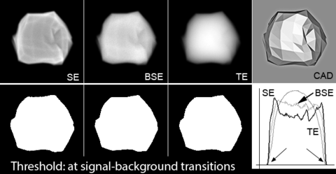
For nanoparticle measurements at 1 keV landing energy, the optimized threshold determined by a physics-based model using a computer aided design (CAD) particle: it is at the signal-background transition for all signals. If the SEM is capable, simultaneous acquisition and the combination of these signals gives the best and quickest results. (SE, BSE, and TE are secondary, backscattered and transmission electron signals, respectively.)
In many cases, SEM measurements are carried out without knowledge of the best measurement conditions, partly due to engineering limits of the SEM, but also due to lack of thorough knowledge of the physics of the signal generation. For example, in many cases the best-quality results can be obtained at (very) low electron landing energies, but the optimal settings are unknown and/or are not possible due to inadequate engineering of the design of the SEM.
It is key that both the signal generation and its acquisition must be optimized to gather the necessary information only in the shortest time. This is only possible through suitable, high-speed, accurate modeling and simulation. Our current modeling software, JMONSEL, is capable of carrying out good-quality model-based nm-scale measurements that are far better than any competing methods that disregard the physics of signal generation. Unfortunately, this software is prohibitively slow for many applications where it could otherwise significantly improve atomic-scale scanning electron microscopy. Even with a larger cluster of general use, CPU-based computers, several months might be needed to carry out a limited set of realistic 2D and 3D simulations of the relevant parameter-space of even a small complex sample.
Fortunately, high-performance, million-times faster modeling and simulation for computational scanning electron microscopy is now becoming possible. Graphical processing units (GPUs) with many thousands of cores (e.g. K80 Kepler by Nvidia) and the CUDA programming environment are available, which are excellent for SEM Monte Carlo simulation. Also, the codes themselves can be improved and optimized so that they will compute the necessary information only—not more, revealing again already known information, which would be wasting time and money; but not less either, which would result in inferior results and a loss of measurement control. We are fostering an international cooperation to usher in the widespread use of computational scanning electron microscopy along with fully optimized, significantly improved, atomic-resolution measurements and new, higher performance SEMs in the future.
Selected Publications
Metrology for the next generation of semiconductor devices, N. G. Orji, M. Badaroglu, B. M. Barnes, C. Beitia, B. D. Bunday, U. Celano, R. J. Kline, M. Neisser, Y. Obeng & A. E. Vladar, Nature Electronics 1, pages 532–547 (2018)
NIST Publication Database Journal Web Site
Research Update: Electron beam-based metrology after CMOS, J. A. Liddle, B. D. Hoskins, A. E. Vladár, and J. S. Villarrubia, APL Materials 6, 070701 (2018);
NIST Publication Database Journal Web Site