
Official websites use .gov
A .gov website belongs to an official government organization in the United States.
Secure .gov websites use HTTPS
A lock (
) or https:// means you’ve safely connected to the .gov website. Share sensitive information only on official, secure websites.
In the growing catalog of nanoscale technologies, nanowires—tiny rows of conductor or semiconductor atoms—have attracted a great deal of interest for their potential to build unique atomic-scale electronics. But before you can buy some at your local Nano Depot, manufacturers will need efficient, reliable methods to build them in quantity. Researchers at the National Institute of Standards and Technology (NIST) believe they have one solution—a technique that allows them to selectively grow nanowires on sapphire wafers in specific positions and orientations accurately enough to attach contacts and layer other circuit elements, all with conventional lithography techniques. They detailed their results in a recent paper.
Despite their name, nanowires are more than just electrical connectors. Researchers have used nanowires to create transistors like those used in memory devices and prototype sensors for gases or biomolecules. However working with objects only tens of nanometers wide is challenging. A common approach in the lab is to grow nanowires like blades of grass on a suitable substrate, mow them off and mix them in a fluid to transfer them to a test surface, using some method to give them a preferred orientation. When the carrier fluid dries, the nanowires are left behind like tumbled jackstraws. Using scanning probe microscopy or similar tools, researchers hunt around for a convenient, isolated nanowire to work on, or place electrical contacts without knowing the exact positions of the nanowires. It's not a technique suitable for mass production.
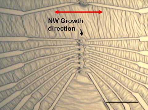
Building on earlier work to grow nanowires horizontally on the surface of wafers (see "Gold Nano Anchors Put Nanowires in Their Place"), NIST researchers used conventional semiconductor manufacturing techniques to deposit small amounts of gold in precise locations on a sapphire wafer. In a high-temperature process, the gold deposits bead up into nanodroplets that act as nucleation points for crystals of zinc oxide, a semiconductor. A slight mismatch in the crystal structures of zinc oxide and sapphire induces the semiconductor to grow as a narrow nanowire in one particular direction across the wafer. Because the starting points and the growth direction are both well known, it is relatively straightforward to add electrical contacts and other features with additional lithography steps.
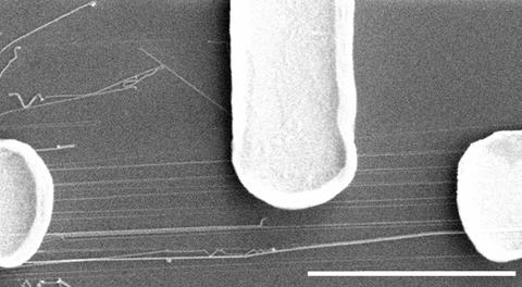
As proof of concept, the NIST researchers have used this procedure to create more than 600 nanowire-based transistors, a circuit element commonly used in digital memory chips, in a single process. In the prototype process, they report, the nanowires typical grew in small bunches of up to eight wires at a time, but finer control over the size of the initial gold deposits should make it possible to select the number of wires in each position. The technique, they say, should allow industrial-scale production of nanowire-based devices.
For more examples of NIST research on nanowire electronics, see: "New Design Developed for Silicon Nanowire Transistors," "Growing Glowing Nanowires to Light Up the Nanoworld," "New Fabrication Technique Yields Nanoscale UV LEDs," "Placing Single Nanowires: NIST Makes the Connection," and "Silicon Nanowires Upgrade Data-Storage Technology."
B. Nikoobakht. Toward industrial-scale fabrication of nanowire-based devices. Chem. Mater., ASAP Article 10.1021/cm071798p S0897-4756(07)01798-X. Web Release Date: October 9, 2007.