
Official websites use .gov
A .gov website belongs to an official government organization in the United States.
Secure .gov websites use HTTPS
A lock (
) or https:// means you’ve safely connected to the .gov website. Share sensitive information only on official, secure websites.
Alternative Computing Group
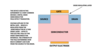
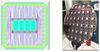
The Alternative Computing Group has two related programs addressing future electronics for information processing. Select an area below for more information.


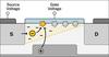
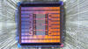
The Alternative Computing Group conducts wide ranging, cross-disciplinary research focusing on innovative measurement science in nanotechnology with an emphasis on applications in future electronics and information processing. Our team consists of physicists and electrical engineers with a broad range of theoretical and experimental expertise. Core competencies include:
Theoretical and experimental device physics research
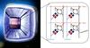
Emerging AI hardware and architectures
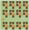
CMOS chip design
Embedded systems for electronics instrumentation
These capabilities combine in research programs that support development of new paradigms in nanoelectronics and computing by advancing measurement science in these areas. The group has programs in hardware for artificial intelligence and CMOS-based measurement platforms, exploring the measurement needs of chip-scale prototyping of novel-device-based technologies.
News and Updates


Projects and Programs

Publications
Awards

Press Coverage
Contacts
Group Leader
-
(301) 975-3721