
Official websites use .gov
A .gov website belongs to an official government organization in the United States.
Secure .gov websites use HTTPS
A lock (
) or https:// means you’ve safely connected to the .gov website. Share sensitive information only on official, secure websites.
Summary
The aim of this project is to develop robust, quantitative measurement methods utilizing transmission electron microscopy methods for complex, nanostructured devices with nanometer and sub-nanometer spatial resolution.
Description
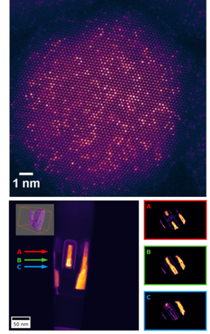
Dark-field scanning transmission electron microscopy (STEM) image (top) of an Er doped CaF2 nanoparticle. In this image mode, the dopant atom locations are indicated by the brigher atomic columns and can be readily identified. (Sample provided by Taejong Paik (University of Pennsylvania)). Dark-field STEM image (bottom left) of tri-gate transistor specimen. Color arrows indicate the location where reconstructions of the 3D structure were extracted (bottom right). Also shown is a volumetric rendering of the full 3D volume (bottom left, inset)
The properties of advance materials are becoming ever more reliant on the ability to manipulate their chemistry and structure at very fine length scales. For example, the relevant feature sizes in state-of-the-art transistors continue to decrease, even as the complexity of the architectures employed increases, and existing characterization methods are proving insufficient for analyzing such devices. Scanning transmission electron microscopy (STEM), with its unique atomic resolution and analytical capabilities, has become a crucial and irreplaceable tool in many industries for the characterization of materials. Instrumental improvements have enabled the simultaneous collection of multiple signals in a single scan and software integration has made it possible to collect more data in an automated fashion.
The focus of this program is the development and application of electron microscopy methods for the characterization of materials at high spatial resolution. This encompasses structural measurements through atomic-resolution imaging and diffraction analysis, as well as elemental and chemical characterization through spectroscopic imaging based on electron energy-loss and X-ray fluorescence. In particular, the program is focused on improving the reproducibility and quantification of such measurements through the development of novel approaches to experimental data collection and processing.
Major Accomplishments
- Artifact free reconstruction of complex three-dimensional architecture of real transistor devices
- Automated alignment and reconstruction methods for quantitative 3D structural and chemical characterization in electron tomography of cylindrical specimens.
- Integration of tomographic data collection and spectroscopic imaging improved material contrast and quantitative analysis in 3D
- Quantitative assessment of active site location in high topography catalyst agglomerates
- Development of a highly-scriptable electron tomography data processing package (https://github.com/usnistgov/tomotools)
- Development of imaging method capable of in-situ tracking of the atomic-scale oxidation state in CeO2 nanomaterials.
- Elucidated the role of certain measurement parameters in quantitative oxidation measurements of CeO2 nanomaterials.
- Integration of high-speed, high-sensitivity diffraction camera to enable four-dimensional (4D)-STEM analysis