
Official websites use .gov
A .gov website belongs to an official government organization in the United States.
Secure .gov websites use HTTPS
A lock (
) or https:// means you’ve safely connected to the .gov website. Share sensitive information only on official, secure websites.
Summary
An urgent objective of the microelectronics industry is to mitigate the extreme heat densities generated within devices that are limiting the performance of next-generation technologies. However, getting the heat from such a localized area of a device to the macroscopic packaging involves many processes that encompass femtosecond to nanosecond time scales—placing impossible demands on current nanoscopic measurement capabilities.
This project will leverage existing high-harmonic generation EUV source to combine ultra-fast time resolution with nanoscale real-space imaging to measure the element-specific dynamics of heat transport in nanostructures and active devices. This measurement advance will provide the critical, and currently unobtainable, feedback for metrology-driven design of next-generation microelectronics and uncover the underlying physics of heat flow at the nanoscale.
Grand challenge 4: Metrology Gaps in the Semiconductor Ecosystem
Description
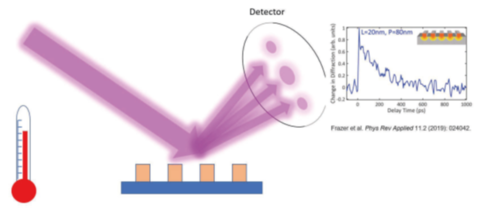
EUV probes a change in diffraction efficiency due to thermal expansion. Time-resolved diffraction provide a measurement of heat flow or the rate of heating/cooling.
Heat is greatly impeding progress in microelectronics, which is only getting worse as dimensions are reduced and device architectures move more towards being 3-dimensional. The dynamics and physics of nanoscale thermal transport are unknown and dynamic measurements of active devices at this scale do not exist. At best, such models are refined using a cumbersome process based on final circuit performance.
The microelectronics industry is therefore forced to rely on finite element models (FEMs) to predict nm-scale heat flow models that are based on many untested assumptions, and which have limited validity at the nanoscale due to their inherent continuum approximation. The continuum model smears out the discrete lattice structure of solids that defines the characteristics of phonons at the nanoscale. The failure of such models has been shown explicitly.
NIST is in a unique position to solve this metrology problem by directly measuring nanoscopic heat flow in structures and active devices.
Circumventing laborious and costly trial and error approach to development would significantly reduce time to market of new technologies. Furthermore, having both validated models and rapid measurement feedback can enable more exploration of innovative and disruptive technology solutions to the heat problem.
This project will fill the metrology void to both provide the measurement to R&D and provide the critical feedback to modeling efforts that seek to predict device performance.