
Official websites use .gov
A .gov website belongs to an official government organization in the United States.
Secure .gov websites use HTTPS
A lock (
) or https:// means you’ve safely connected to the .gov website. Share sensitive information only on official, secure websites.
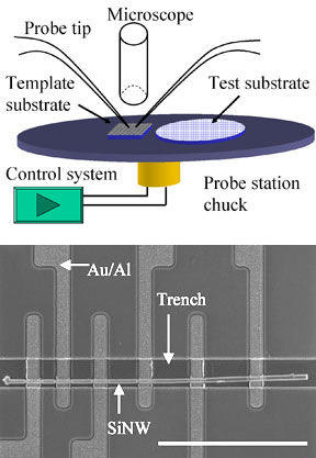
(a) Schematic of NIST single nanowire manipulation system.(b) Scanning electron microscope image shows a single silicon nanowire positioned in an etched trench using NIST's nanowire manipulation technique. The trench helps keep the nanowire in position during the fabrication of the rest of the test structure, which measures metal/nanowire contact resistance. The scale bar is 20 micrometers long.
Researchers at the National Institute of Standards and Technology (NIST) have devised a system for manipulating and precisely positioning individual nanowires on semiconductor wafers. Their technique, described in a recent paper, allows them to fabricate sophisticated test structures to explore the properties of nanowires, using only optical microscopy and conventional photolithographic processing in lieu of advanced (and expensive) tools such as focused ion or electron beams.
Nanowires and nanotubes are being studied intensively as essential elements for future nanoscale electronics, but some fundamentals remain to be worked out—among them, how to put wires only a handful of atoms in diameter where you want them. The smallest-diameter nanowires today are built in a "bottom-up" fashion, assembled atom-by-atom through a chemical growth process such as chemical vapor deposition. This is essentially a bulk process; it produces haystacks of jumbled nanowires of varying lengths and diameters. "The normal research approach," explains NIST electronics engineer Curt Richter, "is to throw a whole bunch of these down on the test surface, hunt around with a microscope until you find a good-looking wire in about the right place, and use lithography to attach electrical contacts to it."
To achieve better control, the NIST engineers modified a standard probe station used to test individual components in microelectronic circuits. The station includes a high-resolution optical microscope and a system for precisely positioning work surfaces under a pair of customized titanium probes with tips less than 100 nanometers in diameter. In a two-step process, silicon nanowires suspended in a drop of water are deposited on a special staging wafer patterned with a grid of tiny posts, and dried. Resting on the tops of the posts, selected nanowires can be picked up by the two probe tips, which they cling to by static electricity. The test structure wafer is positioned under the probes, the nanowire is oriented by moving either the probe tips or the wafer, and then placed on the wafer in the desired position.
Although not at all suited to mass production, the technique's fine level of control allows NIST engineers to place single nanowires wherever they want to create elaborate structures for testing nanowire properties. They've demonstrated this by building a multiple-electrical-contact test structure for measuring the resistance of a nanowire independent of contact resistance, and a simple electromechanical "switch" suitable for measuring the flexibility of nanowires. They've used the technique successfully with nanowires greater than about 60 nm in diameter, and say sharper probe tips and high-resolution microscopes could push the limit lower.
Q. Li, S. Koo, C.A. Richter, M.D. Edelstein, J.E. Bonevich, J.J. Kopanski, J.S. Suehle and E.M. Vogel. Precise alignment of single nanowires and fabrication of nanoelectromechanical switch and other test structures. IEEE Transactions on Nanotechnology. V.6, No.2. March 2007.