
Official websites use .gov
A .gov website belongs to an official government organization in the United States.
Secure .gov websites use HTTPS
A lock (
) or https:// means you’ve safely connected to the .gov website. Share sensitive information only on official, secure websites.
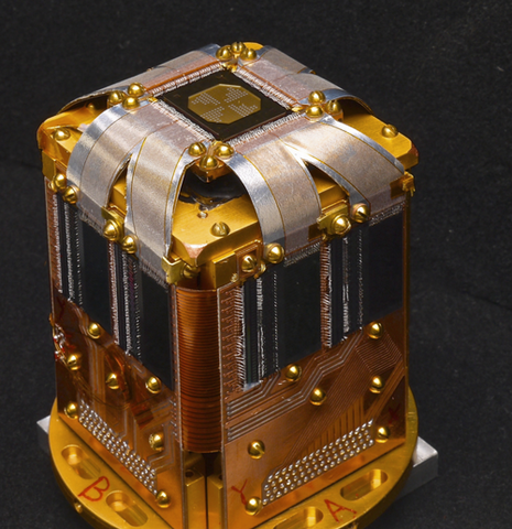
TES detector (at top of device) mounted for use in a beam line.
NIST scientists have pioneered a technology that may speed the arrival of long-awaited materials and devices including advanced high-temperature superconductors and high-efficiency photovoltaic cells: A new high-resolution X-ray spectrometer that was just installed at the Advanced Photon Source (APS), a large facility that produces the brightest synchrotron X-ray beams in the Western Hemisphere.
Certain kinds of materials are investigated using beams of X-rays generated by a synchrotron, in which electrons orbiting a storage ring emit high-energy radiation. A sample is placed in the beam line and then a detector records the X-ray photons that pass through or are scattered off of the sample. The resulting data reveal subtle aspects of the chemistry, structure, and even electrical dynamics of materials – information of critical value to potential developers.
However, "one major problem with conventional technology is that detector efficiencies are typically in the range of 5 to 10 percent," said Daniel Swetz of the Physical Measurement Laboratory's Quantum Electronics and Photonics Division. "That is, they're throwing away about 90 percent of the photons. Moreover, they tend to have poor solid-angle coverage. The X-ray beam is spatially broad, and if you put a small detector in, you won't be using the system most efficiently."
So Swetz, along with Joel Ullom and other NIST colleagues, have been designing and fabricating a new generation of "transition edge sensors" (TESs) that detect nearly 100% of X-ray photons, and can determine energy differences between photons with a resolution of about 1 part in a few thousand at a key energy range for studying materials. That capability is a factor of 50 better than current state-of-the-art detectors and provides highly detailed information about the chemical and electronic structure not easily measurable with other types of spectrometer.
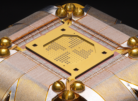
TES detectors, which are a familiar and highly valuable technology in optical physics and astronomy, employ a thin metal film cooled to near absolute zero, which keeps the film on the "edge" between superconducting and normal states. The film sits beneath an absorbing material with high photon stopping power. When an incident photon deposits its energy in the absorber, the heat raises the temperature of the underlying TES film above its superconducting critical temperature and increases its resistance. The resulting electrical signal is proportional to the energy of the photon.
High-resolution X-ray TES detectors have only been employed for about 15 years – following initial research by Ullom and others – and required numerous innovations to reach their current state. In order to record multiple high-energy X-rays at count rates of hundreds per second, materials had to be found that are stable over time, absorb large numbers of photons, are spatially uniform, and that have a very narrow critical transition range.
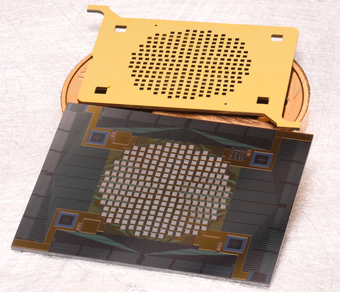
The resulting TES detectors are about 0.1 mm2 and as many as 240 of them are deployed in arrays that currently provide 23 mm2 in collecting area. Current NIST TES detectors are designed to operate at 100 mK using 300 nm thick superconducting bilayers of molybdenum and copper. These devices are fabricated in the new state-of-the-art Boulder Microfabrication Facility on the NIST Boulder campus. In addition, the NIST team had to ensure that there was enough dynamic range in the sensor so that it would not be overloaded by the high energies of X-ray photons, and had to devise a method of tuning the absorption properties by placing a very thin layer of bismuth on top of the sensor to act as the X-ray absorber.
In 2012, the first NIST TES X-ray spectrometer was installed by Randy Doriese and other NIST scientists at the National Synchrotron Light Source (NSLS) at Brookhaven National Laboratory. The success of this first instrument led to a joint project between NIST and scientific investigators at the University of Illinois and Argonne National Laboratory to build a second TES spectrometer for a new beam line under development for the APS. This second instrument was installed this fall and science campaigns are now underway.
At the NSLS, the TES installation dramatically increased the solid-angle coverage and boosted efficiency. "That is particularly important for materials-science measurements," Swetz said, "because the amount of dopant in the sample affects the number of photons of interest that you can see. With higher efficiency, you can probe more dilute samples. And, of course, if you have 100 times the collecting efficiency, you can do measurements 100 times faster."
At the high-intensity APS, the goal is somewhat different. "At the brightest beam lines, the efficiency is certainly desirable," Swetz says. "But what you really need is the ability to separate out the background from your signal. One advantage of our detectors is that because we can distinguish the energy of all the different photons, we can remove most of the noise from the measurement."
The NIST TES systems may also play a significant role in another aspect of X-ray spectroscopy: time-resolved measurements. "People want to understand the dynamics of how charge moves through materials, such as the next generation of photovoltaics," Swetz said. "But we don't understand why their conversion efficiency is so low. If all you have is a static measurement, you don't know where the energy is being lost. However, if you have a sensitive enough detector, you can probe a sample in time. When you excite a photosensitive material with light, electrons begin to move. Then you hit it with X-rays at different time steps.
"By doing that, you can try to understand where the charge is going and why it's being lost. Then presumably you could reengineer the material to boost the conversion efficiency of the photovoltaic."
With the success of these new systems, NIST expects a growing demand for high resolution X-ray spectrometers on synchrotrons and other X-ray materials analysis facilities. Says project leader Ullom, "X-rays are some of the most powerful tools known for the analysis of materials, and investing in novel, highly efficient x-ray detectors is much more cost effective than building larger and brighter x-ray sources."