
Official websites use .gov
A .gov website belongs to an official government organization in the United States.
Secure .gov websites use HTTPS
A lock (
) or https:// means you’ve safely connected to the .gov website. Share sensitive information only on official, secure websites.
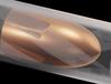
Surface and Interface Metrology Group
Develops and disseminates measurement methods and documentary and artifact standards for the characterization of the optical and topographical properties of surfaces, particularly surfaces and surface finishes important in optical instrumentation, forensics, and consumer products.


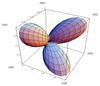
The group’s mission is to maintain the national scales for fundamental optical and topographical properties of surfaces and to advance the state of the art of these measurements. The group works closely with leading U.S. optics manufacturers and metrology instrument manufacturers, government agencies, and academic research institutes to provide new measurement solutions for critical needs. We lead national and international documentary standards efforts that prescribe test methods that ensure product quality and enable global trade. Efforts are undertaken in close collaboration with academic researchers, government agencies, and industry, including stakeholders within the aerospace, forensics, defense, semiconductor, precision manufacturing, and remote-sensing communities. The topographical surface effort realizes and disseminates the SI unit of length for measurements of nanostructure, roughness, waviness, and form for surfaces with vertical dimensions ranging from nanometers to micrometers and horizontal dimensions ranging from micrometers to hundreds of millimeters. Optical properties measurements include index of refraction, surface color and appearance, diffuse and regular transmittance, and diffuse, regular, and angle-resolved surface reflectance.
Calibration Services, Standard Reference Materials, and Documentary Standards
- Standard Reference Materials (SRMs)
- Documentary Standards
The group’s staff actively participate in and lead the development of Documentary Standards on various Standards Developing Organizations (SDOs) by providing the necessary expertise, fundamental measurement science and advanced technologies. We engage with the following SDOs: ANSI-OEOSC, ASME, ASTM, CIE, ISO, and OSAC.
Collaboration Opportunities
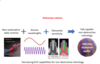
The Surface and Interface Metrology Group welcomes opportunities to collaborate on joint research, technology, and standards development projects to advance the characterization of the optical and topographical properties of surfaces. The group provides multiple opportunities for students, scientists, industry, academia, and other R&D laboratories to collaborate. Specific opportunities depend on current areas of interest within the Group, but may include undergraduate research fellowship, postdoctoral fellowships, visiting scientist, and guest researchers as well as various cooperative research arrangements ranging from formal agreements, such as CRADA, Consortia, and interagency agreements, to informal collaborations. For more details, see Employment and Internship Opportunities and Collaboration Opportunities.
Projects and Programs

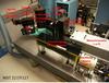
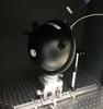
Tools and Instruments


Software
News and Updates


Publications
Awards

Contacts
Group Leader
-
(301) 975-2876
Office Manager
-
(301) 975-6037