
Official websites use .gov
A .gov website belongs to an official government organization in the United States.
Secure .gov websites use HTTPS
A lock (
) or https:// means you’ve safely connected to the .gov website. Share sensitive information only on official, secure websites.
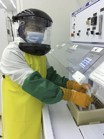
CNST NanoFab intern Patricio Flores in the cleanroom.
When NanoFab intern Patricio Flores donned a bunny suit for the first time last January, he had never been inside a cleanroom or worked with the precision tools that fabricate nanostructures—devices built up of layers only a few atoms thick. Working closely with several NanoFab process engineers, Flores quickly learned how to maintain and prep instruments for researchers from academia, industry and NIST. He also became adept at using software to track the reliability of machines designed to deposit precisely calibrated, ultrathin coatings of metals and polymers on wafers. Soon he was assisting other interns as they learned how to change out the solid material targets that are vaporized and then condense on silicon wafers to form thin films.
Flores’ internship, co-sponsored by the Northeast Education and Technology Education Center (NEATEC) (http://neatec.org/), was only supposed to last four months. But as his internship came to an end, the NanoFab invited him to stay for another four months. Flores, who turned 24 last summer, not only helped other interns as they transitioned from school to the internship, but also compiled a series of standard operating procedures to accelerate the training of the students during their time in the NanoFab.
“Patricio not only assisted in maintaining equipment in the NanoFab, but he also supported process development,” said assistant NanoFab manager Jessie Zhang. “He grabbed every opportunity to learn and improve,” she added.
“Once we worked through the details of a new project, Patricio tackled it independently,” said NanoFab process engineer Jim Bittner, who worked closely with Flores. “He handled new responsibilities reliably and made himself a valuable addition to the operations team by performing daily equipment tasks with minimal oversight,” Bittner noted.
“To see a process through from start to finish was very rewarding,” Flores said.
Off campus, he played as hard as he worked, mountain biking through the Maryland and West Virginia countryside and honing his martial arts skills.
During a job interview at ASML, a manufacturer of advanced semiconductor processing equipment based in Wilton, Connecticut, Flores left nothing to chance. He not only recounted his experience in the NanoFab but gave a PowerPoint presentation on his internship. Last August, to no one’s surprise, ASML hired him as a technician. He works alongside engineers in developing extreme ultraviolet lithography systems critical to the production of integrated circuits.
While at ASML, Flores is also pursuing a master’s degree in mechanical engineering at the University of Bridgeport in Connecticut. As part of his graduate studies, he is helping to develop a robot and payload for a high-altitude NASA balloon.