
Official websites use .gov
A .gov website belongs to an official government organization in the United States.
Secure .gov websites use HTTPS
A lock (
) or https:// means you’ve safely connected to the .gov website. Share sensitive information only on official, secure websites.
Summary
Our multifaceted program provides numerous outputs to assist our customers. First, we develop and evaluate a variety of measurement techniques that provide industry and academia with methods to characterize the chemical, physical, and electrical properties of plasmas. The techniques we develop include improved laboratory diagnostic measurements for use in research and development, as well as more robust, non-perturbing measurements for use in process monitoring and control in manufacturing. Second, we provide experimental data measured under well-defined conditions in highly-characterized standard plasma reactors. Finally, we develop models, which are necessary for gaining understanding and insight into complex plasma properties and behaviors. We rigorously test and validate the models by comparisons with experimental data. Together, the measurement techniques, data, and models help semiconductor manufacturers and plasma equipment manufacturers to better understand and control existing processes and tools and help them to develop new ones.
Description
Intended Impact
The model for rf bias effects that we have developed should make it easier for industry to select optimal operating frequencies and may stimulate the adoption of new methods for RF biasing, such as multiple-frequency bias and non-sinusoidal bias. NIST studies of electrical endpoint detection should enable semiconductor manufacturers to obtain better control of plasma etching processes and other processes that involve rapid changes in wafer surface conditions.
Objectives
Provide advanced measurement techniques, data, and models needed to characterize plasma etching and deposition processes important to the semiconductor industry, enabling continued progress in model-based reactor design, process development, and process control.
Technical Approach
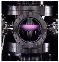
Recent experimental efforts have focused on a new method for measuring electron number density in plasmas, the wave cut-off method. In collaboration with KRISS, the Korea Research Institute of Standards and Science, a wave cut-off probe has been designed and implemented in NIST laboratories. Unlike other techniques, cut-off probes do not suffer from problems with deposition of insulator layers and therefore they are more compatible with real plasma processing conditions.
The cut-off probe has been used to characterize the effect of radio-frequency (RF) bias on the plasma electron density in an inductively coupled reactor. In such reactors, RF bias is used to control ion energies, but it also has unintended effects on electron density and ion flux. Interest in these unintended effects has been stimulated by new methods for RF biasing, such as multiple-frequency bias and non-sinusoidal bias, which make use of frequencies higher than those previously used. We measured the effect of RF bias on electron density over the entire frequency range used in industrial plasma processes. These measurements validated a model that is general and fundamental enough to apply not only in our plasma reactor, but in all inductively coupled reactors. The model makes it easier for workers in industry to select optimal operating frequencies.
We have also performed a fundamental investigation of electrical detection of plasma etching endpoints. In plasma etching, one requires an endpoint signal that indicates the layer being etched is fully consumed, so that the etch process can be stopped before underlying layers are damaged. Electrical signals, such as the voltage or current being drawn by the plasma, are often used to detect endpoint. Unfortunately, the origin of the electrical changes that occur at endpoint are not well understood. Consequently, the electrical signals that are most commonly used, which are chosen for reasons of convenience or based on purely empirical work, are not necessarily the most reliable indicators of endpoint. We performed electrical measurements and simultaneous wave cut-off measurements of electron density during Ar/CF4 plasma etches of silicon dioxide films on silicon substrates. By comparing the electrical data to wave cut-off results and to models of plasma electrical behavior, we were able, for the first time ever, to fully determine the fundamental origin of electrical changes observed at and near endpoint. The work provides recommendations for the plasma etching industry that identify, based on fundamental reasons, which electrical signals are the most reliable for endpoint detection.
Major Accomplishments
- Measured the effect of RF bias on electron density in inductively coupled plasma reactor
- Validated completely general and fundamental model of RF bias effect on electron density
- Determined the fundamental origin of electrical changes at plasma etching endpoint
- Provided recommendations identifying the most reliable electrical signals for endpoint detection
ASSOCIATED PUBLICATIONS
1. Sobolewski, M. A., "In situ measurement of electron emission yield at silicon dioxide surfaces exposed to argon plasmas," Plasma Sources Science & Technology, 30, (2021).
2. Sobolewski, M. A., Wang, Y. C., and Goyette, A., "Velocity boundary conditions for positive ions entering radio-frequency sheaths in electronegative plasmas," Journal of Applied Physics, 122, (2017).
3. Sobolewski, M. A., Wang, Y. C., and Goyette, A., "Ion velocities in the presheath of electronegative, radio-frequency plasmas measured by low-energy cutoff," Applied Physics Letters, 109, (2016).
4. Sobolewski, M. A., Ridgeway, R. G., Bitner, M. D., Sinatore, D., and Hurley, P. T., "Power coupling and utilization efficiencies of silicon-depositing plasmas in mixtures of H-2, SiH4, Si2H6, and Si3H8," Journal of Vacuum Science & Technology A, 32, (2014).
5. Sobolewski, M. A. and Lahr, D. L., "Origin of electrical signals for plasma etching end point detection: Comparison of end point signals and electron density," Journal of Vacuum Science & Technology A, 30, (2012).
6. Sobolewski, M. A., "Origin of electrical signals for plasma etching endpoint detection," Applied Physics Letters, 99, (2011).
7. Sobolewski, M. A. and Kim, J. H., "The effects of radio-frequency bias on electron density in an inductively coupled plasma reactor," Journal of Applied Physics, 102, (2007).
8. Sobolewski, M. A., "Real-time, noninvasive monitoring of on energy and ion current at a wafer surface during plasma etching," Journal of Vacuum Science & Technology A, 24, 1892-1905 (2006).
9. Sobolewski, M. A., "Effects of wafer impedance on the monitoring and control of ion energy in plasma reactors," Journal of Applied Physics, 100, (2006).
10. Sobolewski, M. A., "Noninvasive monitoring of ion energy drift in an inductively coupled plasma reactor," Journal of Applied Physics, 97, (2005).
11. Sobolewski, M. A., "Noninvasive monitoring of ion energy in an inductively coupled plasma reactor," Characterization and Metrology for Ulsi Technology 2005, 788, 319-323 (2005).
12. Steffens, K. L. and Sobolewski, M. A., "2-d imaging of temperature in CF4 plasmas," Ieee Transactions on Plasma Science, 33, 370-371 (2005).
13. Steffens, K. L. and Sobolewski, M. A., "2-D temperature mapping in fluorocarbon plasmas," Characterization and Metrology for Ulsi Technology 2005, 788, 333-337 (2005).
14. Sobolewski, M. A., "Monitoring sheath voltages and ion energies in high-density plasmas using noninvasive radio-frequency current and voltage measurements," Journal of Applied Physics, 95, 4593-4604 (2004).
15. Steffens, K. L. and Sobolewski, M. A., "A technique for temperature mapping in fluorocarbon plasmas using planar laser-induced fluorescence of CF," Journal of Applied Physics, 96, 71-81 (2004).
16. Steffens, K. L. and Sobolewski, M. A., "Effect of changing the electrode gap on the spatial and electrical properties Of O-2/CF4 plasmas," Journal of Vacuum Science & Technology A, 21, 241-250 (2003).
17. Steffens, K. L. and Sobolewski, M. A., "Investigation and control of spatial characteristics of chamber-cleaning plasmas," Characterization and Metrology for Ulsi Technology 2000, International Conference, 550, 233-237 (2001).
18. Sobolewski, M. A. and Steffens, K. L., "Electrical control of the spatial uniformity of reactive species in plasmas," Journal of Vacuum Science & Technology A-Vacuum Surfaces and Films, 17, 3281-3292 (1999).
19. Sobolewski, M. A., Olthoff, J. K., and Wang, Y. C., "Ion energy distributions and sheath voltages in a radio-frequency-biased, inductively coupled, high-density plasma reactor," Journal of Applied Physics, 85, 3966-3975 (1999).
20. Sobolewski, M. A., "Dynamic model of the plasma sheath in high-plasma-density, radio-frequency discharges," International Conference on Phenomena in Ionized Gas, Vol I, Proceedings, 141-142 (1999).
21. Sobolewski, M. A., "Experimental test of models of high-plasma-density, radio-frequency sheaths," Physical Review e, 59, 1059-1072 (1999).