
Official websites use .gov
A .gov website belongs to an official government organization in the United States.
Secure .gov websites use HTTPS
A lock (
) or https:// means you’ve safely connected to the .gov website. Share sensitive information only on official, secure websites.
Analytical Scanning Transmission Electron Microscopy in a Scanning Electron Microscope (STEM-in-SEM)
Summary
Transmission electron imaging and diffraction in an SEM are powerful tools that can be utilized in settings ranging from academia to small business, to semiconductor manufacturing where electron imaging is key to nearly every step of development, production, and testing. It is surprisingly underutilized within the microscopy community, perhaps because the commercially available instrumentation is severely underdeveloped compared to higher-energy electron microscopy tools. To those ends, this project encompasses instrumentation and methodology development for the detection and analysis of transmitted electron signals in SEMs. For example, microstructure, defects, ultrathin film interfaces, nanoparticles, and biomaterial systems are all amenable to qualitative and rigorous quantitative analysis.
Description
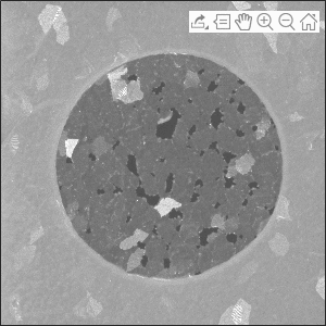
Conventional transmission electron imaging does not necessarily show both strong contrast and high spatial resolution for nanomaterials or soft matter. This is particularly the case for isolated nanostructures or low-Z materials like polymers or biomaterials.
For example, consider structures in the size regime smaller than 10 nm. Electrons with energies of the order of 200 keV exhibit a mean free path for scattering that can easily approach an order of magnitude larger than the structure itself. Decreasing electron energies to those typical of an SEM (~20 keV) reduces the mean free path to values commensurate with the particle size. As a result, more electrons will scatter and the scattering angles will be larger, providing the information-rich content needed to measure crystal phase, crystal orientation, defects, and internal order. A fully analytical STEM-in-SEM has the potential make many powerful TEM-like capabilities available to a large population of SEM users worldwide at a fraction of the cost of conventional higher energy electron microscopes.
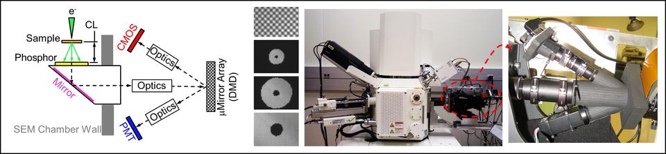
Project activities include development of novel electron detectors and detection schemes, image contrast interpretation, software development to operate instrumentation and interpret results, and proof-of-concept applications to diverse material systems. Regarding detector development, the figure below shows a programmable STEM detector developed at NIST that utilizes a digital micromirror array. This configuration allows both imaging and diffraction in one system. For example, when all the mirrors are flipped to the CMOS camera, diffraction patterns of the sample can be recorded. When user-specified mirrors are flipped towards the photomultiplier tube, a 'virtual' aperture is created that allows real-space images of the sample to be obtained. (Note that post-sample lenses are not required to use specific diffraction spots for dark-field imaging with this detector!)
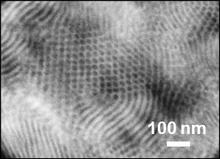
![Au [001] film STEM-in-SEM images, 30 keV](/sites/default/files/styles/480_x_480_limit/public/images/2023/04/11/Au%20%5B001%5D%20defects%20.png?itok=dWDEeKrA)
One strength of this detector is that any combination of the micromirrors can be used to obtain real-space images of the sample by programming different images to the micromirror array. This allows any combination of the transmitted electrons to be used to generate images. For example, defects in an Au [001]-oriented ultrathin film can be highlighted in a straightforward manner by selecting different spots from the diffraction pattern to create bright- or dark-field images with different combinations of virtual apertures. This can be done on the fly by the user or automatically through software scripting as the following images demonstrate.
Aperture automation can be useful in different ways. For example, grain orientation maps of samples such as monolayer graphene or other ultrathin films that aren't amenable to Kikuchi scattering and EBSD characterization can be obtained with this detector. The following three images show a representative 30 keV STEM-in-SEM diffraction pattern obtained from a single grain in monolayer graphene, a set of images that were applied to the micromirror array to implement a rotating array of apertures, and the corresponding set of real-space images associated with the rotating apertures. Notice that different grains appear as the apertures rotate.


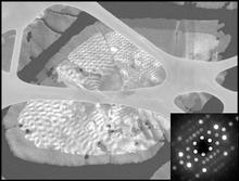
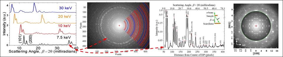
The detector can also be configured as an 'on-axis' camera where the electron beam can be rastered over specific areas of the sample or positioned at specific points to collect various types of diffraction patterns. For example, the following figure shows diffraction patterns obtained at different beam energies from extremely beam-sensitive MFI zeolite nanosheets by rastering a quasi-parallel electron beam (α < 1 mrad) over a large number of nanosheets on an ultrathin carbon support grid. At 7.5 keV, the diffraction peaks are sufficiently well-defined to ascertain lattice parameters on par with hi-res XRD results. The image on the right shows a 20 keV convergent beam [010] zone axis diffraction pattern from a single sheet where the [16 0 0] reflection can be observed.
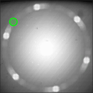
Other emerging transmission electron microscopy techniques can also be implemented in the SEM. For example, 4D STEM is receiving much attention lately. In 4D STEM, a diffraction pattern is recorded at each beam raster position and is stored in a data cube that can be either used offline or online in some cases. There are pros and cons to the technique, but the resulting datasets contain an incredible amount of information that can be useful in many ways. For example, from a basic imaging and diffraction perspective, it is straightforward to collect a dataset and examine the sample offline in real- and reciprocal-space as the following images and diffraction patterns of few-layer MoS2 show.
Major Accomplishments
- Invented t-EBSD (aka transmission Kikuchi diffraction in the SEM), and demonstrated that the important Kikuchi scattering responsible for diffraction appears to occur within a few nanometers of the exit surface of the specimen.
- Obtained t-EBSD patterns from several types of nanomaterials, including HfO2 films of thickness < 5 nm, Fe-Co particles of diameter ~ 10 nm, Pt particles of diameter ~ 2 nm, Fe3O4 particles of diameter ~ 8 nm, Ag particles of diameter ~ 10 nm, Al2O3 particles of diameter ~ 20 nm.
- Demonstrated that t-EBSD measurements can be made over a broad range of film thickness, ranging from < 5 nm to > 3 μm. This can be explained by considering effects of mass-thickness on electron penetration.
- Developed a modular aperture system that significantly improves angular selectivity in the collection of electrons transmitted through a material, as compared to state of the art commercial detectors available today. Acceptance half-angles can be varied from zero to 1350 mrad, with spread controllable to single milliradians, depending on aperture fabrication methods.
- Demonstrated imaging under bright-field, annular bright-field, low-angle annular dark-field, medium-angle annular dark-field, and high-angle annular dark-field conditions – imaging modes typically reserved for the TEM, and until now unattainable as distinct contrast-inducing mechanisms in the SEM.
- Developed a programmable-aperture STEM detector capable of displaying a full diffraction pattern as well as synchronizing a portion of a diffraction pattern with the SEM scan – this results in the ability to generate images associated with any combination of scattering angles, including bright-field, annular bright-field, low-angle annular dark-field, medium-angle annular dark-field, and high-angle annular dark-field conditions. The detector is capable of defining any arbitrary subset of acceptance angles as the basis for imaging.
- Implemented 4D STEM-in-SEM capabilities in an SEM.
- Developed an adapter stage that enables conventional TEM sample holders to be used in an SEM.
B.W. Caplins, J.D. Holm, and R. R. Keller, "Orientation mapping of graphene in a scanning electron microscope," Carbon 149, pp. 400-406 (2019). https://doi.org/10.1016/j.carbon.2019.04.042
B.W. Caplins, J. D. Holm, and R. R. Keller, "Transmission imaging with a programmable detector in a scanning electron microscope," Ultramicroscopy 196, pp. 40-48 (2019). https://doi.org/10.1016/j.ultramic.2018.09.006
J. D. Holm and R. R. Keller, "Angularly-selective transmission imaging in a scanning electron microscope," Ultramicroscopy 167, pp. 43-56 (2016). https://doi.org/10.1016/j.ultramic.2016.05.001
R. R. Keller and R. H. Geiss, "Transmission EBSD from 10 nm domains in a scanning electron microscope," Journal of Microscopy vol. 245, pp. 245-251 (2012). https://doi.org/10.1111/j.1365-2818.2011.03566.x
National Research Council Post-Doctoral Research Opportunities: (you will be leaving NIST website when selecting this link)
Transmission Scanning Electron Microscopy for Materials Characterization
Nanometer-Scale Characterization and Reliability of 2D Materials