
Official websites use .gov
A .gov website belongs to an official government organization in the United States.
Secure .gov websites use HTTPS
A lock (
) or https:// means you’ve safely connected to the .gov website. Share sensitive information only on official, secure websites.
Summary
Most manufacturing has historically been based on top-down fabrication and assembly. With rapid advances in nanotechnology, there is increasing interest in potential construction methods based on self-assembly of nanostructures, particularly approaches incorporating nanoparticles, nanorods, carbon nanotubes, DNA molecules, and block copolymers. The competitive requirement of rapid manufacturing advances will force industry to re-evaluate both traditional and theoretical approaches to nanoscale construction on an ongoing basis, with detailed attention to both the underlying physics and the required metrology. In response to this need, we are developing analytical and numerical models of specific top down and bottom up nanofabrication techniques and processes, as well as models and simulations of their associated metrology challenges.
Description
While self-assembly is still in its relative infancy with respect to practical use, with much additional research required to reach maturity, the more widely utilized top-down methods will continue to require advances and modifications to improve current nanomanufacturing techniques. This modeling and simulation project is therefore focused on the following three areas:
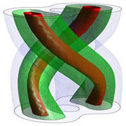
Self-assembly of block copolymers. While fairly well developed in the lab, self-assembly does not have the speed and robustness required for use in mass production nanomanufacturing. Specifically, self-assembled patterns contain errors such as pattern defects and roughness on a scale which is unacceptable for use in industry. In this area, we are working to both understand what drives these errors, and how best to quantifiably measure them. Accurate measurement of such errors are impeded by the limitations of specific imaging techniques such as optical fluorescence microscopy, x-ray scattering, or electron microscopy. We are using self-consistent field theory to model self-assembly processes in order to predict errors and to determine how those errors manifest themselves in x-ray scattering measurements.
Self-assembly is explicitly a nonequilibrium process. For systems in equilibrium there is a well understood standard set of rules describing their behavior. On the other hand general principles for describing nonequilibrium systems are not well developed. Specific nonequilibrium systems can and have been analyzed in detail but we still lack a comprehensive mathematical formalism for describing their behavior. One specific example of a damped driven nonequilibrium system which self-organizes or self-assembles into a coherent state is the laser. This system is extremely well understood and can be analyzed using various mathematical approaches. We are determining whether the mathematical formalism for describing the laser can be extended into a general description of nonequilibrium systems.
Optical microscopy is well developed, robust, and convenient technique for imaging microscopic structures. Unfortunately in the standard mode of operation the resolution is inherently limited by the wavelength of the light used to produce the image. Structures smaller than that wavelength cannot be clearly resolved. However, there are certain cases where the wavelength is not a limitation, such as when researchers need only the relative positions of widely separated nanoparticles. If the microscope optics are either well corrected or well characterized, and it is possible to collect enough light or photons from each particle, then it is possible to locate particle positions with a precision significantly smaller than the wavelength. In spite of the fact that the images of well separated nanoparticles are still blurry, the ability to precisely locate these nanoparticles on a sub-wavelength scale indicates that such an image contains extractable information about the size, shape, and orientation of the samples. Our goal is to determine how to accurately extract this information. To accomplish this goal, we are building an analytical and numerical model using Green's functions to describe how light is scattered from any given nanoparticle or structure and how it is propagated and collected by the microscope to produce an image. The model will be used to quantitatively determine the limitations of measuring the size, shape, and orientation of a given particle or structure as a function of the wavelength(s) used, the numerical aperture, aberrations, illumination pattern of the microscope, and the number of photons collected, among other factors.
Inline metrology for roll-to-roll manufacturing. Roll-to-Roll manufacturing has the potential to very cheaply produce nanoscale features and devices at high speed on a flexible substrate. One example product would be flexible electronics. In concert with the Center for Hierarchical Manufacturing at the University of Massachusetts at Amherst, we are working on developing inline real-time metrology techniques that would be able to monitor the nanoscale patterns as they are being printed. The goal is to be able to determine both the short range and long range coherence of the patterns along with feature size shape and placement. Nanoscale features passing by at up to a meter per second require the metrology system to have a bandwidth on the order of GigaHertz (109 per second). It is not possible to collect and process standard optical images at the rate so we are designing what could be termed "matched optical filters" to reduce the signal processing requirements to acceptable levels.