
Official websites use .gov
A .gov website belongs to an official government organization in the United States.
Secure .gov websites use HTTPS
A lock (
) or https:// means you’ve safely connected to the .gov website. Share sensitive information only on official, secure websites.
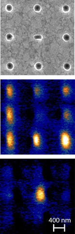
Top: Scanning electron micrograph of an array of magnetic nanodisks with a oval-shaped “defect” structure at center. Middle: Ferromagnetic resonance force microscopy (FMRFM) image of the array at the resonance of a disc. Bottom: FMRFM image at the resonance of the oval.
A team of researchers from the NIST Center for Nanoscale Science and Technology, the Royal Institute of Technology, Stockholm, and the University of Maryland have demonstrated a microscopy method to identify magnetic defects in an array of magnetic nanostructures.* The method represents an important step towards identifying, measuring, and correcting the magnetic properties of defective devices in future information storage technologies.
The ability to detect and understand sources of defects in arrays of magnetic nanostructures is one of the key criteria in the development of future technologies that use the electron spin state to transmit and/or store information ("spintronics"). As in existing information technology, future spintronic devices for information processing will likely require large arrays of magnetic nanodevices with highly uniform magnetic properties; limiting defects will be critical to manufacturing these arrays with tolerable yields. Minute variations in the properties between individual bits will dramatically alter the reliability of the device. Traditional metrology tools such as scanning electron microscopy (SEM) and atomic force microscopy (AFM) can detect geometrical defects but are blind both to buried devices and magnetic properties. Much more information can be obtained through spectroscopic imaging techniques such as ferromagnetic resonance force microscopy (FMRFM), a technique being developed at the CNST that combines the scanned-probe features and buried-device capabilities of magnetic force microscopy with ferromagnetic resonance spectroscopy. In FMRFM, a scanned cantilever probe with a magnetic tip is used to detect magnetic resonances in a sample as it is excited by microwave-frequency magnetic fields from a nearby antenna. These resonances produce small variations in the static magnetization which change the magnetic force on the tip, providing the image contrast.
In the current work, the CNST team used FMRFM to image a magnetic nanostructure array with intentional shape-related defects. In addition to demonstrating that the technique can resolve differently-shaped nanoscale magnetic dots, the researchers were able to measure smaller difference between nominally identical circular dots in the array. The researchers are continuing to improve the new method's sensitivity and spatial resolution, with the long-term goal of enabling wafer-level metrology for future spintronic devices.
*Spectroscopic defect imaging in magnetic nanostructure arrays, H.-J. Chia, F. Guo, L. M. Belova, and R. D. McMichael, Applied Physics Letters 101, 042408 (2012).
NIST Publication Database Journal Web Site