
Official websites use .gov
A .gov website belongs to an official government organization in the United States.
Secure .gov websites use HTTPS
A lock (
) or https:// means you’ve safely connected to the .gov website. Share sensitive information only on official, secure websites.
Summary
A scanning probe microscope (SPM) in its simplest form uses a fine probe tip in proximity to a sample surface to measure a particular physical property. SPMs achieve atomic or nanometer scale resolution using probe tips that have dimensions in this range, and typically measure physical properties by scanning the sample with tip-sample separations of one to a few nanometers using piezoelectric actuators. The advent of scanning probe microscopy in the 1980s led to the birth of the current disciplines of nanoscale science and technology, which focus on measuring and controlling the properties of materials and fabricating new structures at nanometer length scales. The goal of this project is to develop and construct state-of-the-art SPM instruments to advance the state of the art in measurement at the atomic level involving quantum systems and processes. Our current state of the art instruments now contain multi measurements modalities encompassing scanning tunneling, atomic force microscopy, electron spin resonance, and magneto-transport measuring in a single instrument.
Description
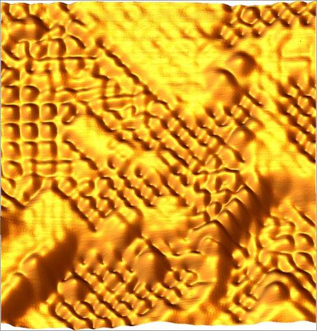
3D rendered STM image of single Er atoms deposited onto a Cu2N surface grown on a Cu(100) single crystal. Image size is 8 nm × 8 nm. The Cu2N regions (corrugated areas) are separated by regions of the bare Cu(100) surface regions (smooth areas). Tunneling parameters: tunneling current setpoint 200 pA, sample bias 10 mV. T = 10 mK.
SPM is a general acronym for various probe instruments. The "P" in SPM stands for various types of probe measurements, such as capacitance (C), force (F), tunneling (T), etc. The scanning tunneling microscope (STM), including custom designs at the CNST, uses the quantum mechanical principle of tunneling between a probe tip and a conducting surface. Force measurements are also currently under development. In STM operation, a fine probe tip is brought to within a fraction of a nanometer from a surface to establish a tunneling current between the probe tip and the surface. The tip is rastered across the surface and the tunneling current is used in a feedback loop to servo the tip position. The measurement of the tip position is recorded as the tip-sample distance and is adjusted to maintain a constant tunneling current. To first order, this raster image yields the surface topography. In addition to topographic features, the STM is inherently sensitive to surface electronic properties due to the dependence of the tunneling process on the availability of electron states. We exploit this sensitivity to measure the surface electron density of states with high spatial resolution, notably for recent measurements on graphene. In certain cases, STM also allows one to selectively image different chemical species. Moreover, we use the STM to fabricate perfect nanostructures on an atom-by-atom basis. Here, an atom is manipulated using the interactions in the tip/sample junction, and moved to a desired location under the control of the STM tip. Our experimental efforts emphasize the custom design of the instrumentation with which we strive to push the frontiers of measurement at the nanometer scale. Within NIST, four custom instruments have been developed for this purpose, briefly described below.
4 K Ultra-high Vacuum Vector High Magnetic Field Scanning Tunneling Microscope
An ultra-high vacuum (UHV) cryogenic STM was custom designed and built as part of the Atomic Scale Characterization and Manipulation Laboratory. The main features of this microscope are operation down to temperatures of 2.5 K inside a superconducting vector magnet cryostat. The vector magnet has a vertical solenoid capable of producing a 10 T field and a horizontal split pair magnet producing up to 1.5 T. Vector operation is computer controlled and can rotate a 1.5 T field in a two-dimensional plane. The microscope system is housed inside an acoustic and electrical shielded room with three stages of vibration isolation. The UHV systems include an MBE system for the growth of materials, a field-ion microscope for tip preparation, and a UHV transfer system to move samples and probe tips through the UHV systems (see Atomic Scale Characterization and Manipulation Laboratory).
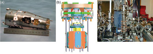
A unique feature of this microscope design is a transportable STM module (Fig. 1a). The STM module contains a three-axis coarse positioning system of the tip-sample junction incorporating 18 shear piezo motor stacks lFig. 1(b)]. The sample is mounted on a vertical piezo translator while the tip is mounted on a two-dimensional, horizontal translator stage that is used to position the probe tip over a specific area of the sample surface. The overall STM module was constructed out of a solid piece of molybdenum to achieve a stiff structural base with good thermal conductivity. The conical shape of the molybdenum module ensures good thermal contact when pressed against a Cu mating cone inside the UHV insert. With this design, we achieve a temperature of 4.3 K. Lower temperature operation down to 2.5 K can be achieved with the aid of a "lambda-refrigerator" inside the cryostat.
The self-contained STM module is translated from the top-loading chamber at room temperature into a vibrational isolated UHV insert that extends into the cryostat [Fig. 1(c)]. When the module is in the top loading chamber, the probe tip can be aligned to a region on the sample with micrometer scale resolution using an optical telescope. This is particularly useful for the study of graphene devices, which can have an active area less than 30 µm wide. The STM module makes electrical contact in the bottom of the UHV insert, where the fixed wiring is routed through a He exchange gas space. The UHV insert is cooled via He exchange gas to avoid vibrations from the boiling of the liquid He in the main bath of the cryostat. This instrument operates exceeding well with high signal-to-noise ratio and is used for a number of projects including: the structure of graphene, magneto-electronic properties of graphene, graphene devices, and atom manipulation.
mK Ultra-low Temperature High Field Scanning Tunneling Microscope
One of the main applications of STMs is to measure the spatial properties of the energy-resolved electron density of states using scanning tunneling spectroscopy (STS), which gives information on the electronic structure of materials. The energy resolution in STS is limited by the operating temperature via the thermal Fermi-Dirac distribution of carriers in the probe tip and sample. Since the initial development of STMs, researchers have pushed instrumentation development to ever lower temperatures to achieve higher energy resolution. The progress to lower temperatures has been slow because of the competing requirements of isolation from the environment for low noise measurements and good thermal coupling required for cryogenic operation. NIST's goal in developing an ultra-low temperature scanning tunneling microscope (ULTSTM) was to design and construct an STM system that operates at ultra-low temperatures (~10 mK) in order to achieve unprecedented resolution in STS measurements of materials and nanostructures for future electronics. The ULTSTM is part of the Atomic Scale Quantum Nanoelectronics Laboratory, which also contains facilities for sample and probe tip preparation.
The ULTSTM instrument development required the integrated research and development of three sub-systems, including a three-stage vibration isolation system, a UHV low noise dilution refrigerator, and an STM module compatible with ultra-low temperatures and high magnetic fields. The vibration system utilizes for the first stage the floating lab floor concept of the NIST Advanced Measurement Laboratory Complex and is part of the Atomic Scale Quantum Nanoelectronics Laboratory. Custom designed second and third stages isolate a granite table and the magnet cryostat system, respectively.
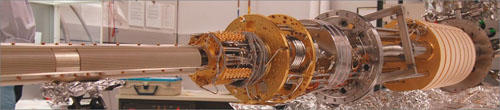
To achieve ultra-low temperatures, a low noise, UHV compatible dilution refrigerator was designed and constructed (Fig. 2). A dilution refrigerator utilizes the circulation, condensing, and pumping of a He3-He4 mixture to achieve millikelvin temperatures. Custom designed features for SPM measurements include all welded and metal sealed construction, a stiff and rigid assembly, a passive Joule-Thompson condenser, and a custom designed mount with electrical connect/disconnect functionality for a transportable STM module. The STM module is similar in design to the 4 K STM described above, except for a smaller size, and use of materials that are compatible with ultra-low temperatures and high magnetic fields. The STM system achieves a base temperature of 10 mK and easily operates at 15 mK with low circulation rates. Current measurements are focusing on future electronic materials such as graphene and topological insulators.
In 2022 the mK STM system was upgraded to a multi-modal measurement system to add atomic force microscopy and magneto-transport measurement capability to operate simultaneously with STM measurement. A new custom SPM module was developed, which incorporates multi-contact sample and tip holders to perform these measurements, as shown in Fig. 3.

Along with the new SPM, extensive RF filtering was implemented for all single lines using homemade powder filters installed on the DR mixing chamber plate, as shown in Fig. 4. This resulted in reaching an electron temperature consistent with the instrument's base temperature of 10-15 mK, as shown in the SIS tunneling measurement in Fig. 5.


Quick Access 5 K Hybrid STM/AFM Microscope
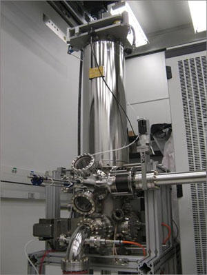
The Atomic Scale Quantum Nanoelectronics Laboratory contains extensive facilities for fabrication of a wide variety of sample systems and probe tip fictionalization. In order to characterize the samples and probe tips before they are introduced into the ULTSTM system, a quick access STM/AFM hybrid system (Fig. 6) was designed and constructed. The system includes a UHV bottom loading cryostat for quick access. The identical STM unit used in the 4 K STM described above is incorporated into this system. The sample and probe tip holders are identical to the ULTSTM system so that samples and can initially be tested in this quick access system and transferred in UHV into the ULTSTM using the linear transfer system of the Atomic Scale Quantum Nanoelectronics Laboratory. The design of the ULTSTM and quick access system incorporate multiple contacts on the sample holder and probe tip holders for atomic forced microscopy (AFM) operation. Specifically a quartz tuning fork AFM capability is integrated into the tip holder so that simultaneous STM and AFM measurements can be performed. Other scanning measurements under design include scanning gate microscopy to investigate electronic device samples in multi-terminal geometries.
Electron Spin Resonance SPM System
The latest SPM instrument was brought on-line in 2025. This new system incorporates four measurement modalities, SPM, AFM, ESR, and magnetotransport measurements in a single instrument operating down to 10 mK. The systems incorporates multiple UHV chambers for MBE growth of thin insulators, field-ion microscopy for probes, UHV rotary transfer system, and a SPM main chamber sitting above the dilution refrigerator (Fig. 7).

The system uses a compact dilution refrigerator with a base temperature of 10 mK and wired for RF excitation down to the SPM module (Fig. 8).

The ESRSPM system uses a new SPM module design where the tip receptacle is fixed in the SPM body and the XYZ coarse and fine motion of the sample is in a self-contained unit. This allows a separate XYZ unit to be placed above the probe to be used for fiber optical measurements of an AFM cantilever. For RF singles, the SPM modules uses SMP connectors at the bottom with flexible RF cables connected to the tip receptacle (Fig. 9).

To accommodate future advances in module design, the system was designed to accommodate multiple modules having different measurement capabilities. These could be picked up and used as needed using a trolly system in the SPM chamber, as shown in Fig. 10.

Selected Publications
- Achieving µeV Tunneling Resolution in an In-Operando Scanning Tunneling Microscopy, Atomic Force Microscopy, and Magnetotransport System for Quantum Materials Research (Invited Article), J. Schwenk, S. Kim, J. Berwanger, F. Ghahari, D. Walkup, M. R. Slot, S. T. Le, W. G. Cullen, S. R. Blankenship, S. Vranjkovic, H. J. Hug, Y. Kuk, F. J. Giessibl, and J. A. Stroscio, Rev. of Sci. Instr. 91, 071101 (2020).
- Invited Article: Autonomous assembly of atomically perfect nanostructures using a scanning tunneling microscope, R. J. Celotta, S. B. Balakirsky, A. P. Fein, F. M. Hess, G. M. Rutter, and J. A. Stroscio, Review of Scientific Instruments 85, 121301 (2014).
- A 10 mK scanning probe microscopy facility, Y. J. Song, A. F. Otte, V. Shvarts, Z. Zhao, Y. Kuk, S. R. Blankenship, A. Band, F. M. Hess, and J. A. Stroscio, Review of Scientific Instruments 81, 121101 (2011).
- A facility for nanoscience research: an overview, J. A. Stroscio, E. W. Hudson, S. R. Blankenship, R. J. Celotta, and A. P. Fein, SPIE, Nanostructure Science, Metrology, and Technology 4608, 112-115 (2002).