
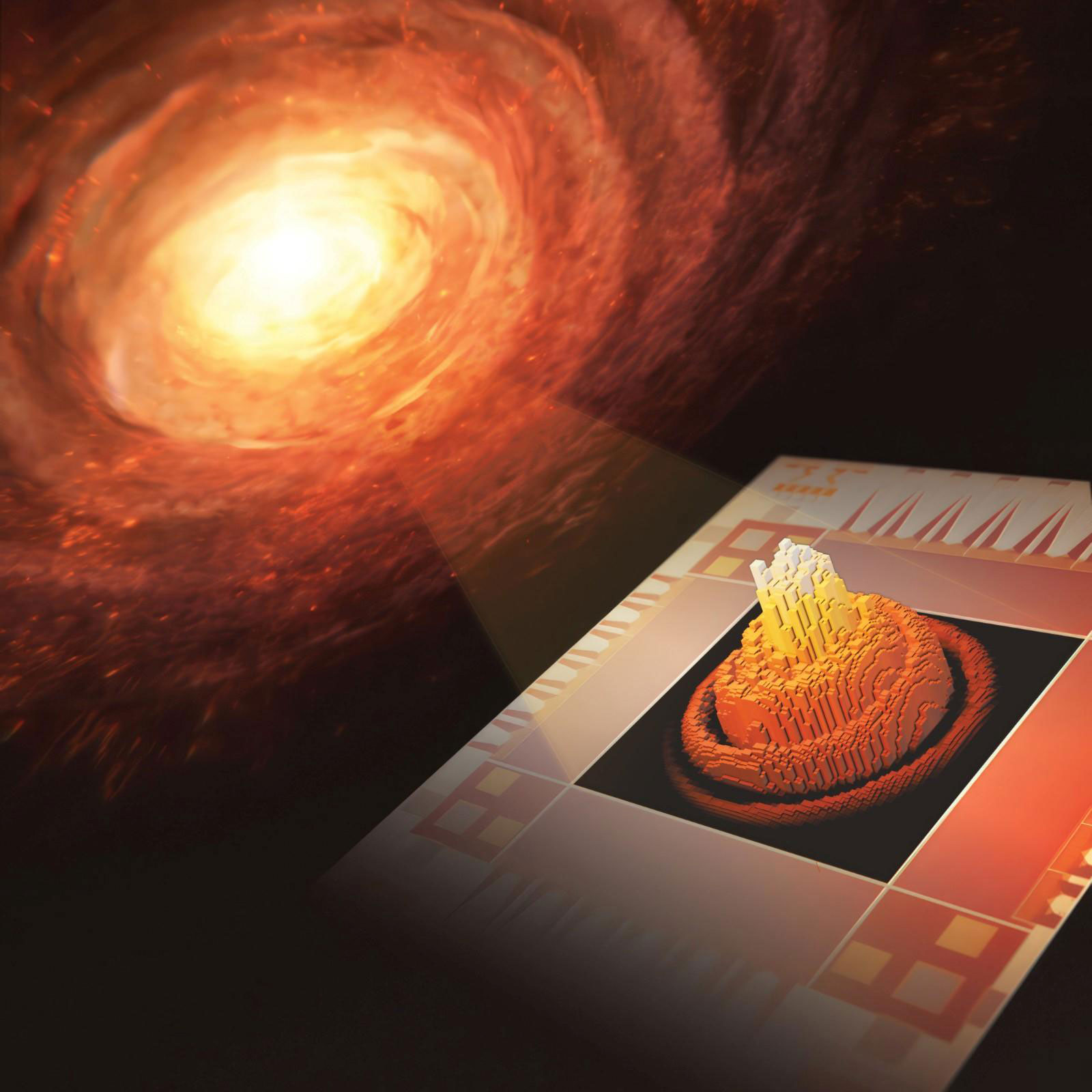
Researchers have built a 400,000-pixel grid of superconducting wires that can detect single photons. Scaled up further, the device could be used to image faint galaxies or brain activity. [Image: pixaby; S. Kelley / NIST]
Scientists have reportedly developed a superconducting camera with over two orders of magnitude more pixels than other similar devices. Their “superconducting nanowire single-photon detector” (SNSPD) uses a grid of extremely narrow superconducting wires held at less than 1 degree above absolute zero to pick up the light from individual photons, registering a dark count rate of only around 1 in a million (Nature, doi: 10.1038/s41586-023-06550-2). They say that the technology, which relies on electrical-to-thermal transduction, is easily scalable and could be applied in areas such as brain imaging and astronomy.
Extreme sensitivity
Superconducting detectors have a number of virtues that make them well suited to picking up exceptionally small amounts of light. Their great sensitivity means that they have very low background noise, so they are able to distinguish even single photons from pitch black almost 100% of the time. They can also operate at extremely high speeds—making detections up to a trillion times per second—while remaining efficient across the electromagnetic spectrum, from the far-infrared up to X-ray frequencies.
However, the detectors’ extreme sensitivity also creates headaches. Among these is the problem of crosstalk between pixels. As a result, scientists have tended to build superconducting cameras by directly tapping the signals from individual pixels. This imposes a limit on the size of such devices, given the need for quite bulky equipment to maintain the superconducting channels at very low temperatures. Until now, no SNSPD had been built with more than about 1000 pixels.
Thermal trickery
In the latest work, Bakhrom Oripov, Adam McCaughan and colleagues at the National Institute of Standards and Technology, USA, together with researchers at the Jet Propulsion Laboratory, USA, have shown that, as with silicon devices, it is possible to build an SNSPD using a grid of superconducting detectors. The researchers managed to serve N × N pixels with just 2N detectors and four “readout buses.” Their trick was to transduce single-photon detections from electrical signals into tiny amounts of heat and then back into an electrical output.
By sending a current through the wires at just below the critical value for that material, they are able to register the transition from resistance-free flow to resistive flow due to the energy deposited by a single photon on any pixel.
The researchers’ grid consists of 500 rows and 800 columns occupying a space of 4 × 2.5 mm, with each pixel measuring just 5 µm on a side. They made the row and column detectors by patterning wires, each just over a micrometer wide, in two 4 nm-thick films of the superconductor tungsten silicide. By sending a current through the wires at just below the critical value for that material, they are able to register the transition from resistance-free flow to resistive flow due to the energy deposited by a single photon on any pixel.
They do this by using the resistance to divert a bias current out of the horizontal and vertical detectors that meet at the pixel in question. That current ends up in a thermal coupler positioned at the end of each detecting wire, yielding a tiny burst of heat that destroys the local superconducting state in another tungsten silicide wire. Four such wires—the readout buses—each run parallel to one side of the grid.
The momentary destruction of the superconducting state in each of the two perpendicular buses yields a pair of voltage pulses that travel at around a third of the speed of light to time-tagger detectors positioned at opposite ends of the bus. The gap between the arrival times of the pulses in each bus then reveals which row and column generated the heat bursts—and therefore which pixel was struck by the photon.
Scaling up
By effectively isolating the signals from neighboring detectors and so largely eliminating the problem of crosstalk, this thermal transduction scheme allowed the researchers to quickly scale up the technology—going from 1,000 to 400,000 pixels in the space of six months. They were able to do so while retaining high-speed and low-background performance, managing more than 100,000 total counts per second compared with just 0.13 dark counts per second.
“The paper was initially written for a 10,000-pixel camera, but we kept revising it as new wafers and better results came in,” Oripov says in comments published by Nature to accompany the research. “After six months, when we got a working 400,000-pixel device, we decided to stop iterating, and to fully characterize the chip and publish the results.”
The researchers say that the work could find a number of applications in the near term, including imaging of microvascular blood flow in the brain and quantum imaging of objects smaller than the diffraction limit.
The researchers say that the work could find a number of applications in the near term, including imaging of microvascular blood flow in the brain and quantum imaging of objects smaller than the diffraction limit. They point out that raising the number of pixels will increase the dead time that occurs in the detectors and read out after each detection, but they reckon that even in very large arrays, the count rates will still be high enough for quantum and biomedical applications.
They add that they will need to improve the system’s detection efficiency and make it workable at wavelengths used in some of the applications they are targeting. They think they can do this by adapting existing optimizations of single-detector efficiencies, and that within about a year, they can build efficient arrays containing a few million pixels to operate at wavelengths such as 1550 nm.