
Official websites use .gov
A .gov website belongs to an official government organization in the United States.
Secure .gov websites use HTTPS
A lock (
) or https:// means you’ve safely connected to the .gov website. Share sensitive information only on official, secure websites.
A new class of tiny chip-based thermometers being developed by PML's Sensor Science Division has the potential to revolutionize the way temperature is gauged.
These sensors, which measure temperature using light, are called photonic thermometers, and compared to traditional thermometry techniques they promise to be smaller, more robust, resistant to electromagnetic interference, and potentially self-calibrating. When fully developed, the designs could be used for remote thermometry, such as being buried into walls or sent into space. They could even be adapted for chemical, pressure, and humidity detection.
Now the PML team that created three promising prototypes for photonic thermometers* has reached a new milestone: they have developed a way to simultaneously connect multiple optical fibers to a chip stably, cheaply, and rapidly.
In the long run, the results may substantially speed up deployment of chip-scale photonic devices and standards by making possible high-volume manufacturing. For immediate purposes, the innovation means that these chip-based sensors are no longer effectively confined to a lab bench: they can now be easily transformed into portable thermometers and submitted to a wider range of tests.
Photonic thermometers work by manipulating light's interaction with structures etched into a chip. For example, one recent prototype uses a feature called a photonic crystal cavity, a waveguide that consists of a silicon strip less than a millionth of a meter in both width and thickness, bored through with holes of varying diameters that scatter incoming light like miniature mirrors. The photonic crystal cavity thermometer acts as a kind of filter for light, with certain frequencies being reflected by the placement of the holes. Which frequencies are scattered depends on the temperature of the chip.
To coax light into and out of a device, researchers use optical fibers, which ferry the light from source to chip and from chip to detector. But for fast testing of multiple devices, the team had always used a lab setup in which the fibers were suspended about a millionth of a meter above the chip. This gap was small enough that the light did not decay much before being caught up again, in a process called evanescent coupling.
Once they had proven that their light-manipulating devices worked, the next logical step was to create prototypes with the optical fibers attached directly to the chip features. And that involved finding a fast, economical way to make a permanent connection.
Attaching individual fibers to chip structures one by one would have been tedious and time-consuming, says PML's Nikolai Klimov, who was tasked with addressing this challenge. To connect multiple fibers at a time, he considered a method that involves bonding an array of optical fibers to the edge of a chip. But this technique would have required the extra steps of precisely cutting off the chip's edge and optically polishing it to ensure efficient coupling. Another downside would have been the somewhat fragile interconnection due to the comparatively small surface area connecting the fiber array to the side of the chip, which in this case is a mere 0.7 mm thick.
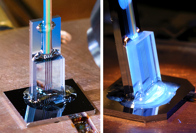
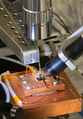
Instead, Klimov developed an effective but relatively simple solution. He used a commercially available optical fiber array, which comes assembled in a block with a set spacing between adjacent fibers. He then designed and built a photonic chip with the same set spacing between the adjacent light-collecting photonic structures.** Using a custom-built platform with six degrees of freedom and the ability to make position changes of less than a millionth of a meter at a time, he carefully aligned the fiber array with the light-collecting photonic structures on top of the chip, and held it in place with a droplet of UV light-curable transparent epoxy.
The result is a thermometry "package" that consists of a photonic chip with its integrated temperature-sensing devices, and an array of optical fibers bonded to the top of the chip like a ponytail.
Although their first package uses an array that contains only 4 optical fibers, the method could be scaled up as much as 12 times by using off-the-shelf arrays that contain as many as 48 optical fibers in a block. Using arrays with many fibers will allow the researches to easily and reliably package multiple photonic devices and sensors on a single chip.
In addition, the researchers found that light leakage at the fiber-to-chip interconnection is minimal, giving them as good quality a coupling as they had with their "suspended fiber" setup, which they say is reasonable for a high-quality measurement and sufficient for many applications.
So far they have tested the new photonic thermometer packages from 10 to 80 degrees C, and neither the epoxy nor the fiber-to-chip bond has shown any signs of degradation. In the next few weeks they will continue to evaluate the packaged thermometers at a wider range of temperatures, from -40 degrees Celsius to 150 degrees Celsius, to ensure that the epoxy holds.
They also plan to explore various types of adhesives for the fiber-to-chip bonding, which could allow them to use a packaged photonic chip at cryogenic temperatures – all the way down to 4 degrees Kelvin (4 degrees above absolute zero).
-- Reported and written by Jennifer Lauren Lee
_________________
*See "Lighting the Path to Smaller, Tougher Thermometers" and "Device to Measure Temperature (and More) with Light".
**The light-collecting photonic structures in this case are grating couplers, which could be described as acting like funnels that take the relatively large-diameter light beams propagating through the optical fibers and feed them into the much thinner on-chip waveguides connected to the thermometry devices. The core of a typical optical fiber is about 8 micrometers (millionths of a meter) in diameter. By contrast, the on-chip waveguides are only about 500 nanometers (billionths of a meter) wide and 220 nanometers thick, so the area of their cross section is almost two thousand times smaller.