
Official websites use .gov
A .gov website belongs to an official government organization in the United States.
Secure .gov websites use HTTPS
A lock (
) or https:// means you’ve safely connected to the .gov website. Share sensitive information only on official, secure websites.
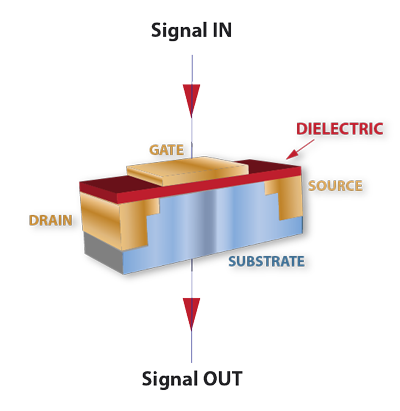
A diagram of a transistor showing where the signal enters and where it is collected in both charge pumping and the new frequency-modulated charge pumping (FMCP).
Until recently, the semiconductor industry had a go-to method for quantifying atomic-scale defects in the billions of transistors contained in a single computer chip. This favored technique, called charge pumping, helped semiconductor manufacturers maintain the quality of their chips, and was used by industry researchers to test the viability of new designs or materials for the next generation of transistors.
But about a decade ago, industry leaders were forced to abandon the use of charge pumping as a side effect of the shrinking sizes of transistors.
At the urging of industry leaders, NIST scientists from the Physical Measurement Laboratory's (PML) Semiconductor and Dimensional Metrology Division, in partnership with colleagues from academia and industry, recently created a new version of this once popular technique that works even for extremely thin transistor components. The method is called frequency-modulated charge pumping (FMCP),* and semiconductor industry leaders have already begun sending staff to NIST in preparation for implementing the technique at their own facilities.
Charge pumping reveals the relative number of atomic-scale defects such as broken bonds and missing atoms, which drastically reduce a transistor's performance and reliability. These defects are also called "interface traps" because they form at the interface between two key parts of a transistor: the semiconductor channel through which the transistor's current flows; and the gate dielectric, which acts as a kind of barrier that blocks charge from entering the channel except when the gate is switched on.
Though industry researchers have other methods for inferring the number of defects at this interface, charge pumping was a favorite because it was "inexpensive, easy to use, and particularly suited to the quantification of these interface traps," says PML's Jason Ryan who co-developed the replacement technique.
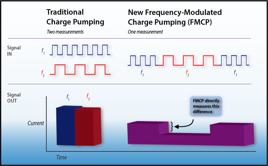
Traditional charge pumping involved essentially alternating between filling the traps with electrons and then draining them. A researcher would apply a voltage to a single transistor's gate. That voltage had a square waveform**, which means it transitioned between two voltages extremely quickly with little time spent ramping up or down. The frequency at which the voltage alternated was usually anywhere from thousands to millions of times a second (kilohertz, kHz, to megahertz, MHz).
The key to assessing the number of traps at the interface was to take this measurement multiple times with a different frequency each time. The reason was that the amount of charge that could be collected from the interface traps depended in part on the frequency of the waveform of this applied voltage. (See graphic.) Each resulting signal was measured as direct current.
Trouble arose, however, as transistors shrank. A thick gate dielectric "barrier" does its job well: it prevents current from leaking to the semiconductor when the transistor is off. But as the dielectric layer became thinner to allow for smaller and smaller transistors, those leakage currents grew. And unfortunately, traditional charge pumping picked up the leakage currents along with the charge pumping signals.
At first this was not a deal-breaker: it was believed that the gate leakage current "noise" was the same for a device no matter what frequency was applied, so researchers continued to make their measurements at multiple frequencies and then edit out the noise through post-measurement processing. But eventually, dielectric layers became so thin, and their corresponding gate leakage currents so large, that this workaround lost its efficacy.
"The fundamental problem was that we were measuring a very small signal buried under a huge background," Ryan says. A typical chip might have transistors that yield a charge pumping signal a thousand times smaller than the leakage current.
The new frequency-modulated charge pumping (FMCP) relies on the same basic concept as traditional charge pumping: researchers alternately fill and drain the interface traps with electrons by applying a gate voltage (MHz or kHz) to a transistor at two or more different frequencies. But instead of applying multiple gate voltage waveforms to the device one frequency at a time, taking direct current measurements, and analyzing them offline, in FMCP a single gate voltage waveform is applied to the transistor, and that single waveform is modulated back and forth between two or more frequencies. Alternating between different frequencies hundreds of times per second allows for a more precise measurement of a small signal by transforming charge pumping into an alternating current measurement.
According to Ryan, semiconductor industry representatives seem eager to have a version of charge pumping back in their toolbox.
"It's easy, and it uses only devices and tools that semiconductor manufacturers would already have in their labs," Ryan says. "It's simple but very effective."
In developing the new technique, the PML researchers also discovered a hidden source of error that may improve future versions of FMCP.
Previously, it was understood that a transistor's leakage current was the same no matter what frequency of voltage was applied to the gate. This assumption is a foundation for both traditional and frequency-modulated charge pumping measurements. But the team found that in fact the leakage current does change slightly depending on what frequency of voltage is being applied.****
Even with this information, however, Ryan says FMCP is still qualitatively useful for assessing the density of defects in the interface, since the error has only a small effect on measurements. The team has proposed several workarounds and will continue to examine this phenomenon in the coming months.
-- Reported and written by Jennifer Lauren Lee
*Jason Thomas Ryan, Jibin Zou, Richard Southwick, Jason Paul Campbell, Kin P. Cheung, Anthony S. Oates, and Ru Huang. "Frequency-Modulated Charge Pumping with Extremely High Gate Leakage." IEEE Transactions on Electron Devices, Vol. 62, No. 3, March 2015. DOI: 10.1109/TED.2015.2395956.
**A waveform in this case is a physical representation of the voltage being applied to a transistor's gate per unit time.
***This leakage is due to a quantum phenomenon in which charged particles tunnel through the dielectric even when the gate is in "off" mode. For advanced devices in which the dielectric layer is only 1-2 nanometers thick, the tunneling probability becomes very high, leading to large amounts of leakage current.
**** The error comes from the fact that no square wave is perfectly square; it always has a finite rise and fall time. Higher-frequency waveforms spend a greater proportion of their time rising and falling (i.e. more transitions per unit time) compared to lower-frequency waves.