
Official websites use .gov
A .gov website belongs to an official government organization in the United States.
Secure .gov websites use HTTPS
A lock (
) or https:// means you’ve safely connected to the .gov website. Share sensitive information only on official, secure websites.
Angela Hight Walker of PML's Semiconductor and Dimensional Metrology Division and colleagues have succeeded in measuring a previously unknown but essential property − thermal conductivity −of an ultra-thin material that is expected to play a major role in the fast-emerging field of nanoelectronics.
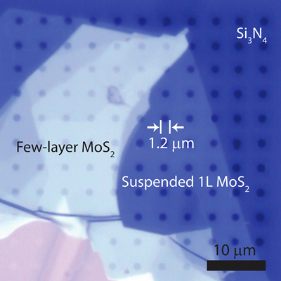
A brief animation shows the experimental set-up, in which a monolayer of molybdenum disulfide is placed atop a perforated grid. Then laser light is applied to the sample over one of the perforations, ensuring that the recorded thermal conductivity of the sample is unaffected by contacting materials.
The compound is molybdenum disulfide (MoS2, or "moly" for short), one of the so-called 2D materials – those in which one dimension is only a few nanometers thick. The first and most famous member of this class is graphene, the chicken-wire-shaped array of carbon atoms isolated only a decade ago. That accomplishment was the basis of the 2010 Nobel Prize in Physics. Such materials are of increasingly urgent interest to researchers and industry for use in advanced electronic device structures with feature dimensions measured in nanometers (billionths of a meter) that can read, write, and store data in ways quite different from conventional transistors.
A number of 2D materials "are exhibiting properties that may enable new memory devices," according to the just-released International Technology Roadmap for Semiconductors, the industry guidebook for future innovation. Moly, a substance made up of alternating layers of molybdenum and sulfur, each only one atom thick, shows promise for data-storage miniaturization beyond the current levels of flash memory. But until very recently, one of moly's key attributes had never been measured.
"At the time we began our study, little was known about the thermal properties of this material," Hight Walker says, "and yet that information is crucially important Measurement of thermal conductivity is an absolutely critical step in the evaluation of a material for applications in electronics – or anywhere else, for that matter."
In a publication earlier this year, the team reported the first measurements of thermal conductivity in moly monolayers – not just with samples supported on substrates such as sapphire, or interacting with electrical insulators such as hafnium oxide, but on isolated samples of moly suspended in space over open areas about 1.2 micrometers wide and thus unaffected by the thermal properties of the contacting materials.
"What makes this work particularly significant," says Hight Walker of the Nanoelectronics Group, "is that we are now able to really probe the intrinsic physical properties of the material. Scientifically, this is very exciting."
The team used a technique called Raman spectroscopy, which involves shining monochromatic laser light on the atomically thin moly sample and detecting the scattered light. The frequency of the scattered light depends on the way the material stretches and vibrates, and during imaging temperature affects these vibrations.
The group studies the effect of temperature two ways: one by heating the sample environment, and one by increasing the laser power onto the sample. The researchers were able to determine that moly is about 100 times less efficient at conducting heat than graphene, but that its thermal response can be modeled quite well.
The new measurements provide the first comprehensive look at how moly is affected by temperature rise caused by electrical current, light, or other sources. The findings may hasten the use of moly – alone or in combination with other 2D materials – in new electronic devices, or other anticipated uses such as water-splitting for hydrogen generation and improved electrodes for lithium-ion batteries. "By understanding what its properties are, we can match it with applications to leverage the wonder of the material," Hight Walker says.
A wide range of applications is contemplated. "Although two-dimensional (2D) transition metal dichalcogenides (TMD) have been studied for decades, recent advances in nanoscale materials characterization and device fabrication have drawn significant attention in the semiconductor industry due new opportunities for 2D electronic and optoelectronic devices," says Gennadi Bersuker, Fellow at SEMATECH.
"With the range of attractive properties such as presence of a band gap and high thermal and mechanical stability, TMD materials have opened up new opportunities for a wide variety of applications including low-power digital and flexible electronics, sensors, photovoltaics, and spintronics."
Collaborators on the project included scientists from Notre Dame and Towson University as well as the Ecole Polytechnique Federal de Lausanne in Switzerland, which provided the extremely high-quality MoS2 samples. The work was conducted at PML laboratories in Gaithersburg, MD, which have the sophisticated equipment and instrumentation required to make the precision measurements.