
Official websites use .gov
A .gov website belongs to an official government organization in the United States.
Secure .gov websites use HTTPS
A lock (
) or https:// means you’ve safely connected to the .gov website. Share sensitive information only on official, secure websites.
Nanoscale Functional and Structural Characterization of Thin-Film Inorganic Solar Cells
Summary
Large-scale implementation of solar power generation requires photovoltaic (PV) devices with efficiency-to-cost ratios better than existing silicon-based solar devices. Next generation devices depend on new materials and device structures. Thin-film PV devices, also called Second Generation devices, while becoming competitive with Si-based technologies, face unresolved technical challenges in achieving their potential for high efficiency. Additionally, the current generation of commercial thin-film solar cells based on cadmium telluride (CdTe) or copper indium gallium (di)selenide (CIGS) incorporate relatively rare elements that might become the limiting factor for wide scale deployment. New photovoltaic devices based on earth-abundant elements are actively being sought. All devices based on inorganic thin films feature sophisticated microscale and nanoscale material structure, grain boundaries, and defects that can be either beneficial or detrimental for the overall device performance.
In this project, we are developing measurement tools and techniques to characterize the physical processes related to light absorption, energy transfer, and carrier dynamics in thin-film inorganic PV materials and devices.
Description
In photovoltaic cells, light absorption creates free excitons that subsequently separate into free electrons and holes under the influence of the electric field of a p-n junction. In first generation cells, light absorption is achieved with an indirect bandgap material (Si) with low quantum absorption efficiency, whereas second generation cells rely on direct bandgap materials (including CdTe and CIGS) and consequently have significantly relaxed criteria on the required thickness for efficient light absorption. To generate useful power, the free carriers must leave the PV device and reach their respective contacts. Although the thickness of second generation cells, and consequently the required carrier diffusion lengths, are roughly two orders of magnitude smaller than Si-based cells, the efficiencies of these second generation cells remain below those of Si cells. This shortcoming is primarily associated with the enhanced charge trapping and reduced lifetime of carriers caused by the significant defect-induced recombination of compound semiconductors. Metrology capable of identifying charge trapping states inside thin-film PV materials, heterojunctions, surfaces and contact interfaces and of determining their impact on device performance could significantly contribute to PV development efforts.
Grain boundaries are important defect structures in thin-film PV materials. Their role, their microscopic structure, and their impact on carrier recombination, transport and device performance are not fully understood. It is possible that certain properties of the grain boundaries that are very sensitive to processing conditions are the critical factors defining the PV device performance.
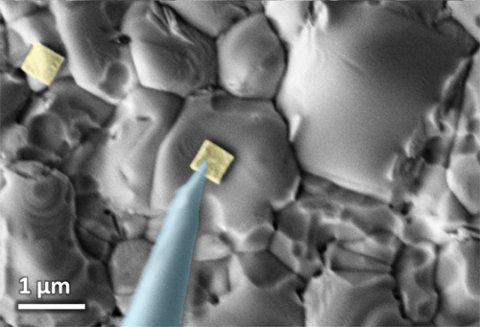
We are exploring different experimental approaches to characterize the functional properties of thin-film PV devices at the spatial scale of single grain or grain boundaries to correlate these with their structure at nanoscale and atomic resolution. The first specialized tool is based on a field–emission scanning electron microscope equipped with electrical nanoprobe and Electron-Beam Induced Current (EBIC) and Cathodoluminescence (CL) measurement systems. Using prefabricated nano-contacts (as seen in the figure above), we can interrogate the electrical properties of grains and grain boundaries. We can also measure local carrier generation, recombination and extraction efficiency, drift, and diffusion across the grain boundaries. Another measurement setup is based on a modified scanning probe instrument equipped with broadly tunable light source. We study photocurrent generation on the nanoscale, collecting current either from nanocontacts or using an AFM tip with various conductive coatings, in order to understand the correlation between the local structure and the collection efficiency in PV materials The data are used to build effective models relating nanoscale material properties to macroscopic PV device performance.