
Official websites use .gov
A .gov website belongs to an official government organization in the United States.
Secure .gov websites use HTTPS
A lock (
) or https:// means you’ve safely connected to the .gov website. Share sensitive information only on official, secure websites.
Summary
At the heart of nanotechnology is the need to create nanostructures, which are material structures whose dimensions are in the nanometer scale. Typically, nanostructures have new properties that differ from their parent macroscopic material due to their small size. These new properties can be harnessed to create new applications, such as quantum dots, small nanometer sized spheres with specific light absorption properties that can be used in drug delivery applications. Future advances in nanotechnology require more precise control of the fabrication of nanostructures. The ultimate goal of nanofabrication is to develop the ability to place a single atom at any given location to create any desired structure. A spectacular achievement involving the ability to manipulate a single atom became possible using the scanning tunneling microscope (STM). The goal of this project is to develop advanced STM techniques to manipulate single atoms to create desired nanostructures and to develop measurement methods that lead to an increased understanding of the atom-surface interactions in order to improve the efficiency of the atom manipulation process.
Description
Manipulation of single atoms with the scanning tunneling microscope is made possible through the controlled and tunable interaction between the atoms at the end of the STM probe tip and the single atom (adatom) on a surface that is being manipulated. In the STM tunneling junction used for atom manipulation, a host of interactions that depend on the electric potentials between the sample and probe tip, the tunneling current, and tip-adatom distance come into play in the atom manipulation process. Understanding and optimizing these interactions is central to improving the efficiency and reliability of atom manipulation needed for large-scale construction of atomic scale devices. Part of the goal of this project is to develop measurements that are sensitive to the atom manipulation process. In the CNST we have developed a number of advanced measurements to "see" and "hear" the atom movements, which we then use to develop advanced atom manipulation systems, including an autonomous atom assembler.
Measuring the atom manipulation process
To image a single atom, the STM places the probe tip sufficiently far from the sample (about 1 nm) so the tip does not disturb or interact with the atom that is being probed. As shown in Fig. 1, imaged cobalt atom remains stationary. In the very good microscopes developed at the CNST, the same single atom can be studied for many weeks or even months due to the ultra-clean and ultra-stable low-temperature microscope environments. In order to move a single adatom, we bring the tip closer to the adatom by adjusting the tunneling junction resistance (the junction resistance is set by the ratio of the tunneling voltage to the tunneling current). With the STM we can control the tip-adatom distance with incredible precision, measured in picometers (1 trillionth of a meter), so we can bring the tip to just shy of contacting the adatom. One can think of the atoms of the tip and adatom getting so close as to start to form a chemical bond or trapping potential, due to the electrons from each atom overlapping each other. This "tunable" chemical bond can be adjusted by setting the tip-adatom distance.
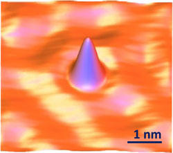
Fig. 1 STM topographic image of a single Co atom on Cu(111) shown in a light shaded view. Current 1 nA, sample bias -10 mV, T = 2.3 K.
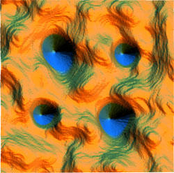
CNST researchers developed a new measurement method of the atom manipulation process we call a "manipulated atom image". For a standard image, the tip height is measured as it is scanned over the atom. A collection of such scans is then combined to form the image (Fig. 1). To create a manipulated atom image, an atom is trapped below the tip by tuning the tip-adatom bonds as described above. The tip height trace is then measured during the rastering of the tip over the surface, as in the normal STM topographic image, except now the adatom is trapped in the moving tip-induced potential trap. Details on the scale of a fraction of a lattice constant are observed in the manipulated atom image, as shown in Fig. 2(a). Our understanding of the manipulated atom image follows from the dynamics of the adatom motion hopping between two different lattice sites in the Cu(111) lattice, which are the fcc and hcp sites. The manipulated atom image for cobalt on Cu(111) can be thought of as a binding site image for the cobalt atoms, with the additional contrast changes between the fcc and hcp sites yielding information concerning the difference in the potential energy for these two sites. Using the motion of the cobalt atom to image the local binding sites and give information on the local surface potential is an example of a new class of measurements based on single atom transducers sensing local environments, which we refer to as an "atom based metrology".
We can gain insight into the atom dynamics from a quantitative measure of the noise properties of the tunneling current. To measure the current noise, we measure the time dependence of the current at the hcp site in a manipulated atom image Fig. 2(b). The tip is paused during the raster and the STM feedback is opened. The tunneling signal is then measured as a function of time for several values of the tunneling bias voltage. Random telegraph noise (RTN) can be seen in these measurements. The RTN signal corresponds to the cobalt atom switching between the hcp site (the higher current signal) and nearby fcc sites (lower tunnel signal). When the tip position is near the center of the hcp site, the cobalt atom is observed to switch to all three neighboring fcc sites. As the tip is biased towards one of the fcc sites, only two-states are observed in the RTN signal corresponding to the cobalt atom switching only to one fcc site. In this way, an ideal two-state fluctuating system can be created based on the position of a single atom using the tip-adatom interaction, which allows the detailed study of the atom switching mechanisms.
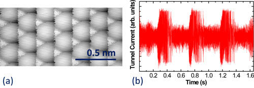
Fig.2 (a) Manipulated atom image of a cobalt atom over the Cu(111) surface. Tunnel current, 50 nA; sample bias, −5 mV; T = 4.3 K. The labels A, B, and C denote fcc, hcp, and top sites, respectively. (b) Tunnel current recorded during manipulated atom image going through the hcp and fcc sites as indicated by the horizontal red line in (a). The increased noise in the tunnel current corresponds to the position of the hcp sites.
Autonomous atom assembly
The ability to use an STM to move and position atoms with lattice site precision provides us with a "quantum" workbench to study the effects of both the electronic structure and of quantum confinement on perfectly built nanostructures. So far, atomic manipulation has been performed manually, or with rudimentary computer assistance. CNST researchers are working to extend this capability by developing an Autonomous Atom Assembler (AAA). Built by adding hardware and software extensions to our low temperature STM system, the AAA will be capable of assembling a desired nanostructure from an unknown random collection of atoms without human intervention. During the AAA's operation, a dilute coverage of adsorbate atoms will be deposited on a clean, flat substrate. The AAA will then instruct the STM to image the random adsorbate pattern to identify the position of each adsorbate atom relative to the substrate lattice, and to plan a series of probe tip moves to place the available atoms at positions specified in a previously entered diagram. The plan minimizes construction time, follows a set of extensible rules, and allows for error correction. The AAA then instructs the STM to execute the plan and, upon completion, provides an image of the final assembled nanostructure. In our initial trials, cobalt atoms were deposited at sub-monolayer coverage on a Cu(111), forming a random pattern of atoms. Using the AAA system, we constructed a variety of nanostructures. Figure 3 shows the autonomous assembly of the NIST logo nanostructure. The ripples in the Cu surface originate the fluid-like electron "waves" in the Cu surface bouncing off the cobalt atoms. When the adatoms form a closed pattern, the bouncing waves can form dramatic patterns, as shown in the quantum elliptical corral in Fig. 3. These special wave patterns lead to new electron energy levels, which may form the basis of nanotechnology applications.
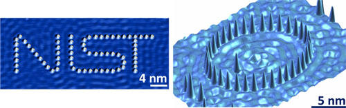
Fig. 3 (left) NIST logo nanostructure fabricated with cobalt atoms on a copper surface with the autonomous atom assembler. The ripples in the background are due to electrons in the fluid-like layer at the copper surface bouncing off the cobalt atoms, much like the patterns produced when pebbles are dropped in a pond. (right) Elliptical quantum corral fabricated with cobalt atoms on the Cu(111) surface using the CNST developed autonomous atom assembler.
Selected Publications
- Invited Article: Autonomous assembly of atomically perfect nanostructures using a scanning tunneling microscope, R. J. Celotta, S. B. Balakirsky, A. P. Fein, F. M. Hess, G. M. Rutter, and J. A. Stroscio, Review of Scientific Instruments 85, 121301 (2014).
NIST Publication Database Journal Web Site - Electronically induced atom motion in engineered CoCu nanostructures, J. A. Stroscio, F. Tavazza, J.A. Crain, R. J. Celotta, and A. M. Chaka, Science 313, 948-951 (2006).
NIST Publication Database Journal Web Site - Controlling the dynamics of a single atom in lateral atom manipulation, J. A. Stroscio and R. J. Celotta, Science 306, 242-247 (2004).
NIST Publication Database Journal Web Site