In AZoM's latest interview, we talk with Jeff Shainline from the NIST in Boulder, CO, about his research looking at forming superconducting circuits with synaptic behavior.
Please can you introduce yourself and your professional background?
My name is Jeff Shainline. I’m a physicist at the National Institute of Standards and Technology (NIST) in Boulder, CO. I was trained as a device physicist, originally working primarily on photonic devices. In the last decade, I’ve moved more into the intersection where electronics and photonics meet—optoelectronics. In particular, I see extraordinary opportunities where superconducting electronics, semiconducting electronics, and photonics all contribute unique physical attributes to powerful, heterogeneous systems.
What are some of the key limitations that current computer systems face?
Current computers are all based on silicon transistors. Transistors can do a lot of things, but in modern computers they primarily act as binary switches, on or off, zero or one. This is the foundation of digital computing. If the operations you want to perform are well represented by binary information, silicon microelectronics are going to be very successful for that problem. Doing mathematics, storing large datasets, performing long, logical procedures—these types of tasks are performed very well by existing computers.
Our current computers also have a certain architecture, where the processor is separate from the main memory, so computation and memory access are separate processes. There is a communicate link between the location where memory is stored and the location where the information pulled from memory is used in the processor. This is called the von Neumann architecture, and it dates back to the 1940s. It remains the standard because it is much simpler and cheaper to fabricate processors and memory chips separately.
These two aspects of modern computers—their underlying binary operations and their von Neumann architecture—bring strengths and weaknesses. They can be extremely fast, cost-effective, and versatile for a wide range of tasks that can be reasonably represented by binary digits, particularly if those tasks don’t require an intimate interplay between memory and processing. The weaknesses are felt when these conditions aren’t met. If the information is not well represented by binary digits and/or if the type of computation requires extensive interplay between processing and memory, other computational devices and architectures can bring advantages.
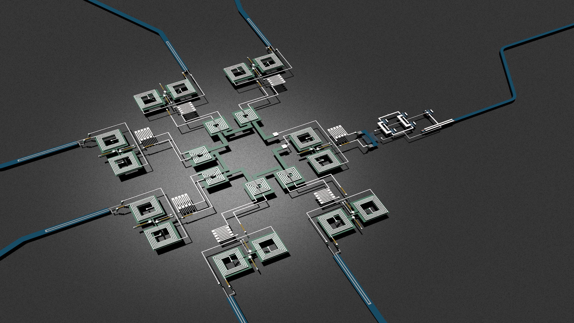
Circuit layout of a small superconducting optoelectronic neuron. Waveguides deliver photonic signals to superconducting detectors. A semiconductor light source couples spike events to an outgoing waveguide.
For example, imagine looking at a natural scene, perhaps walking in a forest. There may be bright and dark regions, many different colors, all manner of shapes and edges. Rather than representing this information as a long list of zeros and ones to specify different quantities at different pixels, it is more efficient to represent this information with analog signals that can take many values across a certain range. It is more efficient to ignore almost all of the information, and just draw attention to certain aspects, such as distinct edges and boundaries of objects. Rather than storing a megabyte of information that lists the value of pixels in a big blue object, it is more efficient to be aware that everything up there is the sky, and it’s blue.
When memory and processing are intertwined, conventional computers may not be the best choice. Our brains do this amazing thing that is called associative memory. If you see a small part of an object or hear a small fragment of a word or song, your brain quickly fills in the rest. As the brain begins to process the initial fragment, memory is accessed that completes the object or song.
The physical structures that are responsible for processing and memory are not separate in the brain. This becomes very important for learning, which is a key aspect of intelligence. Our brains learn efficiently in part because the act of processing information engages and can update memory. When memory and processing are separate, as in the von Neumann architecture, the communication link that connects the two domains becomes the primary bottleneck of the system. One must constantly read and write, sending information back and forth. The brain avoids this by not separating memory and computing. Memory and computing devices are broadly distributed across the brain in an extraordinary network with extensive interconnectivity in much more of a web configuration than a box-and-arrows configuration. This allows information to be processed, memory to be retrieved and written, and communication to be carried out between all components rapidly and efficiently.
What drove you to look to the human brain for inspiration in improving upon these limitations?
I think it is natural to look to the brain for inspiration. It’s sitting right there on top of each of us. Actually, I’m amazed by digital computers as well as the brain. I think it is astonishing that digital computers can perform extensive, exact mathematical calculations far faster than any human ever could. It is equally astonishing that a human can quickly glance out at a scene or at another person’s face and immediately understand exactly what is going on in some much larger context with a great deal of nuance. I think the most comprehensive intelligent machines will embody capabilities from across this spectrum. However, at present, we have extremely good digital computers based on silicon microelectronics, and we do not have particularly strong machines based on the principles of brain computation. So there is more to do in that area.
If we look at how the brain processes information and really try to soak up the lessons from neuroscience, we find that our computational systems must evolve at the basic device level all the way up to the system architecture level. Silicon transistors are a crucial tool in the toolbox, but they shouldn’t be used for everything. Superconducting components like Josephson junctions have much to offer when we try to perform the operations of synapses, dendrites, and neurons. Similarly, communication at the scale of the vast networks of the brain is much more feasible and scalable when light is used instead of electrical signals. I was driven to look to the brain for inspiration because it is the only known computational hardware that can achieve general intelligence, rapid learning, and the cognitive functions that allow us to hold this big picture of what the world is and how it all relates. But upon looking further into how this is all accomplished, I—and many others—realized there is a huge need and therefore opportunity to add additional devices and physical mechanisms to our computational toolbox in addition to transistors.
In the past, ‘neuromorphic chips’ have been developed that use brain-like software. What are these and what issues with them caused you to look even further?
Neuromorphic chips exist along a spectrum. Some chips are nearly identical to digital computers at the device level, still using silicon transistors and binary digits to represent everything, and only departing from conventional processors at the level of the architecture and the communication protocol. Examples of this approach include IBM’s TrueNorth chip and Intel’s Loihi chip. They’re digital chips, but memory—though still separate from processors—is more broadly distributed across the system. These chips communicate by sending spike events from each processor to many others, more like neurons in the brain that communicate with spikes sent from each neuron to thousands of synapses. So some neuromorphic chips leverage the very same devices, hardware, and fabrication infrastructure as conventional digital computers, but they are processing information in a way that is based on the spiking neurons and distributed architecture of the brain. This is quite a sensible thing to do, because you can get going already. All the infrastructure is already there.
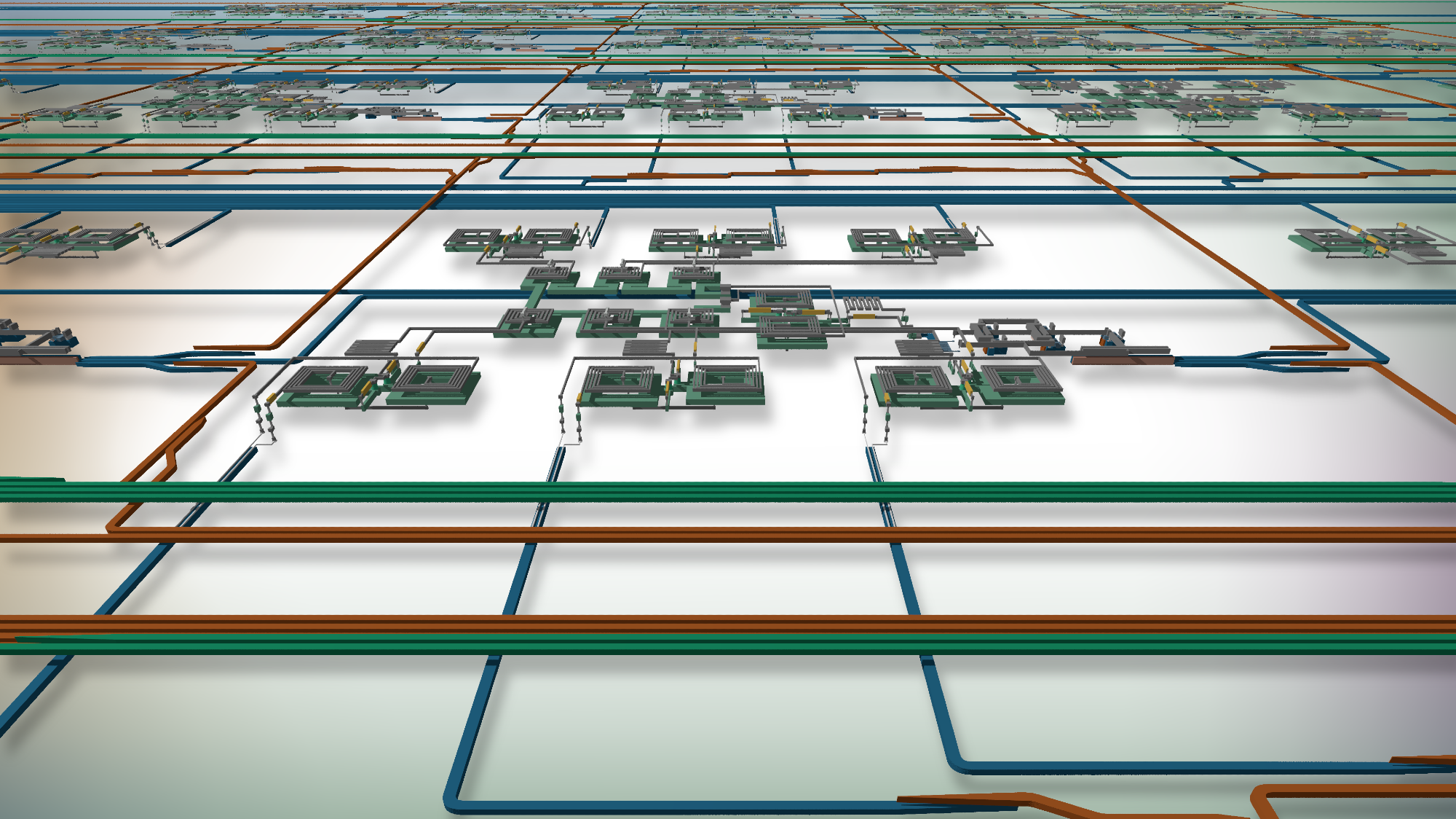
Network of many optoelectronic neurons and multiple planes of interconnecting waveguides.
On the other end of the spectrum, there are neuromorphic chips that go even further and use silicon transistors as analog devices, taking another page from the book of the brain. Instead of binary, on-off signals from transistors, these efforts use transistors in what is called the “sub-threshold” regime in which the current through the transistor can take a continuum of values as a function of the applied voltage. This can lead to dramatic energy savings. The problem here is that the functional form of the current through the transistor is exponential, meaning a small change in the applied voltage or a small change in the fabrication of the transistor leads to a large change in the current response.
This strikes me as a sub-optimal analog computational primitive because it is quite difficult to connect many such devices into circuits that work well together. Realization of a dendritic tree—the part of a neuron that accumulates and processes signals from the synapses on the way to the neuron cell body—is very difficult with these analog devices that have an exponential response.
The shared problem of nearly all neuromorphic chips at present is the communication between neurons. In the brain, when a neuron spikes, it sends a signal along what is called an axon. This axon branches to deliver the information to thousands of synapses. The signal is able to maintain its strength across the entire branching axon due to the brilliant, self-assembled nanotechnology from which we are all constructed. The signal regenerates as it propagates, and it can do this because the neuron is embedded in the extracellular medium, which continually supplies the needed charge—ions—to regenerate the signal. It is extremely difficult and energetically inefficient to accomplish the same feat with transistors and copper wires.
If the output signal of a neuron is generated by a transistor, it is not possible for that transistor to source enough current to drive a long, branching copper wire up to a voltage that will cause the thousands of recipient synapses to register the event. So instead, the neuromorphic community has come up with a clever workaround. Neurons do not make direct, dedicated connections to their downstream synapses. Instead, each neuron only makes a connection to a node in a communication network. This communication network then handles the spikes sent between all neurons.
This form of communication is much more like packets being sent across the internet than it is like spiking neurons sending messages over axons in the brain. Such a communication method has been a key enabler of existing neuromorphic systems because if you are trying to use the circuits that are fabricated in an existing silicon microelectronics process, there isn’t another option. However, the problem is that this shared communication infrastructure does a reasonable job up to a certain scale—maybe about a million neurons (our brains have 86 billion neurons)—but beyond that, it gets bogged down. It takes too long for a message sent by a neuron to arrive at its synaptic destinations, particularly when many other neurons fire closely in time. The latency to send a message depends on the traffic on the network. This is the primary impediment to scaling existing neuromorphic systems, and this was the starting point that led to our work on photonic communication between spiking neurons.
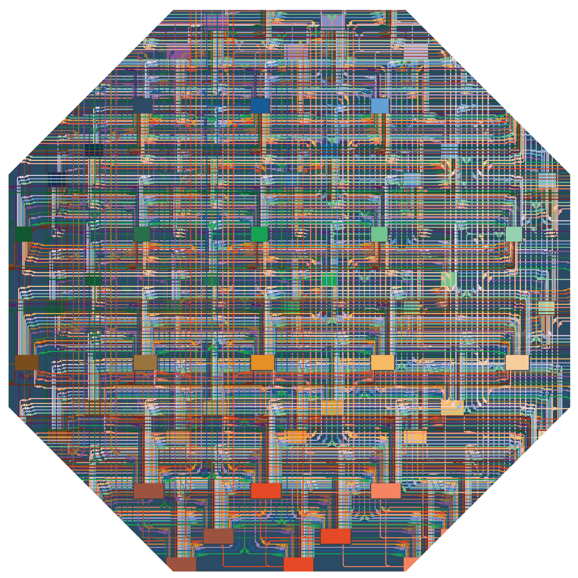
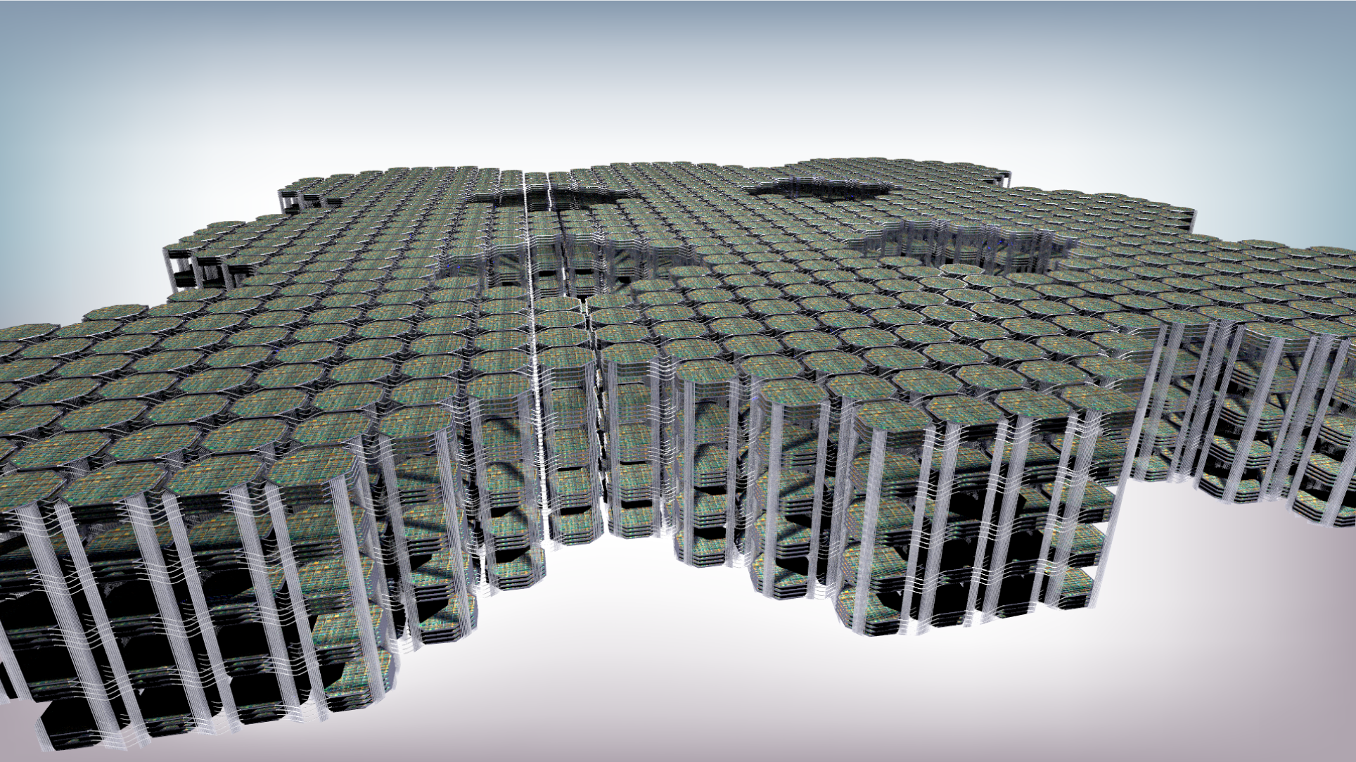
Schematic illustration of a wafer-scale optoelectronic network. To achieve brain-scale systems, neuromorphic hardware will require densely integrated networks combining multiple wafers interconnected by fiber optics.
It’s important to emphasize here that none of the shortcomings of existing neuromorphic chips are due to poor decisions by the people developing this technology. It is perfectly sensible to make spiking neural networks with the existing hardware infrastructure that was developed for digital computing. It is perfectly sensible to try to use transistors as analog devices. It is not the engineers’ fault that transistors have an exponential response function in analog mode. It is not the engineers’ fault that transistors cannot activate a thousand synapses. All of these challenges and limitations are due to basic physics, not poor judgement. That is what we are trying to do—bring additional physics into the hardware we use for brain-inspired computing.
You have designed networks that allow a circuit to behave like a synapse. Could you explain how you were able to achieve this with single-photon detectors?
Yes, our original objective was to overcome the limitations of the shared communication infrastructure on neuromorphic chips using photonic communication instead of electrical communication. With light, it is possible for one neuron to send spike events to thousands of synapses, each with a dedicated connection, without the need for a shared communication infrastructure. In principle, one could do this with more conventional optical links, such as those used to send information between servers in data centers over optical fibers. The problem is that integrating the light sources typically used for such applications with the electronics that are used for computing has proven to be extremely difficult, despite significant resources being brought to the problem for several decades. This is because light sources are usually based on semiconductors such as GaAs which have a very different atomic spacing than Si, so they cannot be easily grown on the same wafer. GaAs light sources are required because Si doesn’t emit light at room temperature.
Another problem is related to the detectors that receive the light. It’s difficult to design optical links that require fewer than a thousand photons without power-hungry amplifiers. If a neuron needs to send a few thousand photons to a few thousand synapses in a brief time window, this is actually pretty demanding for the optical link. Our group at NIST developed these single-photon detectors based on superconducting devices. Now, instead of requiring a few thousand photons to register a pulse, we could do it with just one—a single photon to communicate from a neuron to a synapse.
This was very intriguing, but we needed a way that this optical detection event could lead to an electronic signal that could then be used in the computations performed by synapses, dendrites, and neurons. We considered many approaches to this problem, but as soon as we started working with circuit designs that combined single-photon detectors with Josephson junctions, everything clicked in place. A Josephson junction is a circuit element based on two superconducting wires separated by a thin insulating barrier. They have beautiful properties and are used in superconducting electronic circuits for many applications from particle detection to voltage standards. All the neuromorphic functions we needed were sitting right there, ready to be harnessed.
It was a pretty natural choice to combine superconducting single-photon detectors with Josephson junctions. We designed the circuits and laid out a bunch of experiments we wanted to try. We were able to get the fabrication working quickly because our team at NIST already had the single-photon detector process dialed in, and our collaborators (also at NIST) had the Josephson junction process figured out. My colleague Saeed Khan and I came up with a strategy for how to interface the two processes, and it worked the first time we tried it. That was nice.
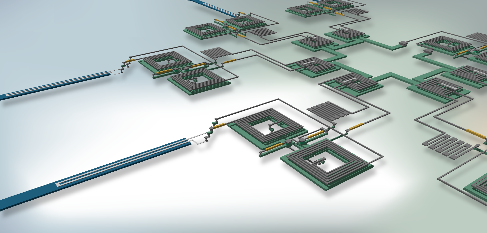
Single-photon synapse. A superconducting single-photon detector is integrated with a nanophotonic waveguide. The output of the detector is coupled to a superconducting circuit that performs computational operations analogous to a biological dendrite
One of the key aspects of this approach to synapses is that it works at the single-photon level. Once you have decided to send signals with light, you cannot send a fainter signal than one photon, which means this is the energy-efficiency limit. This is very important for scaling. But if you want to send the most energy-efficient messages from a neuron to its synaptic recipients, you still need a way to change the synaptic weight, which is the amplitude of the signal generated by the communication event. Since you are only sending one photon per connection, the amplitude of the signal cannot be set by the amount of light you send, and even if it could you wouldn’t want to do that because it would defeat the efficiency benefit of single-photon communication.
The key aspect of the synapse circuit that allows this to work is that we can change the synaptic weight in the electrical domain using Josephson junction circuits. One single photon comes in, strikes the detector, and that drives current into a Josephson junction. Then, the amount of current generated on the other side of that junction is determined by the current bias to that junction. The current bias is basically the electrical drive line. So adjusting this electrical parameter controls how much current is generated by the photon-detection event, and this represents the synaptic weight. That’s how the detectors and Josephson junctions work so well together.
One other aspect to mention is that these detectors and Josephson junctions are based on superconductivity, so they have to operate at low temperatures around 4 kelvin. This is 200 times warmer than quantum computers but still requires specialized systems to keep the devices cold. This adds system complexity, but it also brings tremendous benefits. I mentioned earlier that it has proven incredibly challenging to integrate light sources with silicon electronics since silicon doesn’t emit light at room temperature. However, when we work at low temperatures, silicon does emit light, so one of the major impediments to progress in optoelectronic systems—the lack of a silicon light source—is overcome when we embrace superconductivity and work at low temperatures. Because we have single-photon detectors at each synapse, the silicon light sources can be quite faint and still get the job done. This is a tremendous advantage for system scaling that outweighs the inconvenience of low-temperature operation.
How does this technology compare to previous and current standard systems?
Our approach to neuromorphic computing is very different than current standard systems for many reasons. As I’ve emphasized, we’re using light for communication and superconductors for major parts of neural computation. The vast majority of current systems use semiconductor electronics for all of them. We still use semiconductors to interface our superconducting neurons to our light sources when a neuron fires a spike, but the high-speed, energy-efficient analog computations are performed by superconducting circuits forming synapses, dendrites, and neurons. Superconducting circuits are so much more naturally equipped to perform these functions, and they do so much faster and with less energy than their semiconductor counterparts.
Large neuromorphic supercomputer combining many wafers of densely integrated superconducting optoelectronic circuits.
There are other efforts using photonics for communication in neural systems, but they typically try to use light for some of the computation in addition to the communication. For example, most other efforts using light for communication try to establish the synaptic weight based on the amplitude of the optical signal. This is very costly from an energy perspective because light requires more energy to generate than electrical signals—especially when compared to superconducting electrical signals. I’m not aware of any other teams using light in conjunction with superconductor electronics. The other teams using light for communication in neural systems are, to my knowledge, all trying to work at room temperature, and as I said above, this means they have a serious challenge integrating light sources with their electronic circuits, and their detectors require thousands of photons per synapse event. It would be nice to work at room temperature, but when all factors are taken into consideration, it actually looks much more difficult than at low temperature. This only becomes apparent when you think at the scale of large systems.
There’s another community that is fine with working at low temperature, but they don’t want to have to deal with photonics in their systems. These folks are trying to make full spiking neural networks using superconducting circuits alone. This is a worthwhile objective, and great progress is being made. But we’re staying the course with optoelectronic systems because all of our scaling analyses indicate that the performance of a communication infrastructure built on superconducting electronics alone will lag far behind an optical interconnect fabric for large-scale systems. Just like in the case of semiconductors, this communication becomes the primary bottleneck that limits the scale of neural systems the hardware can achieve.
So our approach is unique in that we are combining semiconductors, superconductors, and photonics to make the best use of each for the physical attributes they offer. We have looked very closely at how we might proceed by leaving any one of the legs off of this three-legged stool, and we conclude the system suffers. Yes, it is more complicated to fabricate wafers that have all three physical attributes working together, but the performance benefits are myriad. And we’re an intrepid bunch, so here we go.
What applications could this technology revolutionize?
In 1943, Thomas Watson, the President of IBM said, “I think there is a world market for maybe five computers.” That estimate was incorrect, and we now know that computers are absolutely everywhere doing everything. Some might say that because our systems require cryogenic cooling the application spaces will be limited. This is true: superconducting optoelectronic hardware will not be in your phone. But our systems take roughly the same volume of space as an air conditioner and use less power, and air conditioners are in many homes around the world. So it is entirely feasible that these systems will become integrated into many aspects of daily life because they will be more intelligent and faster than any other way of pursuing the same computations.
Our team is currently focused on the application of video processing, where the temporal dynamics of spiking neurons bring efficiency and speed benefits. Major internet companies have to analyze the content of millions of video uploads every day, and the current techniques for doing this have unsustainable costs in terms of energy and time. Our networks will do far better.
Many applications beyond this will also be revolutionized. These include medicine and individualized health care models; insurance pricing and risk assessment; logistics, such as the routing problems associated with package delivery; high-speed signal processing for 5G and 6G networks; and neuroscience, where this sophisticated technology may help us better test hypotheses related to the functioning of our own minds.
In the more distant future, the major strength of this technology is that it can continue to scale up to networks with more neurons and synapses than our own brains while operating a quarter million times faster. It will take a long time to get there, but what applications will we find for AI with intelligence far exceeding our own? “Applications” may be the wrong word when we look that far ahead.
What limitations must be overcome before this technology can be scaled up? What are the next steps?
At present we’ve demonstrated all the components of our hardware, but we have not realized the full fabrication process with all components integrated together on a single wafer. That is the primary challenge we’re focused on right now. Our team at NIST is small, so this is a significant undertaking. To be scaled up, this project will need to transition to industry. The next step would be to spin out a startup, get investors interested, and grow our team, but that is perhaps a conversation for another occasion…
What is the most significant or exciting part of this research to you?
As we get deeper into these systems we keep discovering more reasons why this approach is so powerful. All of our theoretical analysis indicates that systems of immense scale, complexity, and speed will be achievable. Realizing them will be an extraordinary technological achievement, but it will be feasible with a reasonable level of investment, and the benefits to society could be immense. It is extremely exciting to work on something with such potential and to work with a team that continues to get more passionate as we see our experiments succeed as planned.
But “exciting” and “significant” are two different things. The most significant part of this research is how it extends into the future, potentially transforming not just AI but much of what we do with computers.
And even beyond that—it looks completely physically possible and practically feasible to construct artificial cognitive systems vastly beyond the scale and complexity of our own brains while operating on dramatically faster timescales. If correct, this will change what we mean by intelligence, it will change our conception of ourselves as the smartest creatures on the planet, and it will change our conversations around what we are doing here on Earth.
That will be a significant turn of events.
Where can readers find more information?
Our website can be found at http://www.soen.ai.
More from AZoM - Papertronics: Disposable Electronics on a Single Sheet of Paper
About Jeff Shainline
 I’m currently with the National Institute for Standards and Technology where my role is the leader of the Physics and Hardware for Intelligence Project. Before I joined NIST I worked with a great team to demonstrate optical communication between a processor and memory in a digital computer. That work is described here. That early career highlight enforced the idea that using light for communication in computers will be valuable and practical. Once I moved to NIST, I began working with my current group in which superconducting single-photon detectors are a large part of what we do. My original goal was to develop integrated systems based on photons for quantum information processing, but I quickly became convinced that the hardware we were developing was much better matched to a new implementation of neuromorphic computing. We elaborated on the underlying concepts in a 2017 paper and refined the details in a 2019 paper. A key milestone was the demonstration of an optical communication link at the single-photon level, combining silicon light sources with superconducting single-photon detectors. Because it was based on silicon light sources, that work gave us confidence that our superconducting, single-photon approach to neuromorphic computing would be able to scale to very large systems. Recently, we added the next element to our synapses: Josephson junctions, the most important superconducting element. By combining Josephson junctions with single-photon detectors, we were able to demonstrate the key processing functions of synapses and dendrites, including synaptic weighting in the electronic domain, temporal integration, and memory retention across a broad range of timescales. Now we have demonstrated the key components and we are ready to build systems that solve problems and bring value to the world.
Disclaimer: The views expressed here are those of the interviewee and do not necessarily represent the views of AZoM.com Limited (T/A) AZoNetwork, the owner and operator of this website. This disclaimer forms part of the Terms and Conditions of use of this website.