U.S. flag

An official website of the United States government

Official websites use .gov
A .gov website belongs to an official government organization in the United States.

Secure .gov websites use HTTPS
A lock ( ) or https:// means you’ve safely connected to the .gov website. Share sensitive information only on official, secure websites.

Atom Scale Device Group

Develops, measures, understands and exploits quantum and electronic devices and sensors at the interface between atomic and nanoscale solid-state systems. Systems under study include dopant-based and nanofabricated Si devices for quantum technologies, quantum simulation, quantum sensing and charge sensing, spins in nanoscale and atomic scale solid-state systems, and hybrid solid-state systems.

Our program combines theory and experiment. Theory is extending the fundamental understanding of systems at the atomic/nanoscale interface, probing the frontier between the classical and the quantum, exploring new applications in nanoscale and quantum technologies, and motivating new, precision metrology. We are developing the theoretical understanding needed to exploit nanoplasmonic and semiconductor quantum dot structures for quantum and nanoscale technologies, to develop next generation atomic clocks, to simulate exotic condensed matter with ultracold atoms, to understand quantum information propagation in interacting systems, and to implement useful quantum information, detection and measurement protocols.

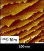
Experiment is being conducted to develop precision measurement tools for this regime, to collect precise data essential for the applications mentioned, and to further the understanding of these systems. We are probing the charge and spin transport, optical, and mechanical properties of nanoscale and quantum-coherent solid-state systems. We are exploiting nanoscale Si devices to provide precision charge sensing on-chip. We are exploring the use of these nanoscale Si devices for quantum technology and are pushing these devices to the atomic scale using structures fabricated by controlled placement of individual dopants. Such devices will allow us to explore the ultimate atomic-scale limit for traditional Si electronic devices and implement atomic-scale quantum technologies in Si. We are developing isotopically enriched Si needed for Si quantum technology and investigating novel materials for spintronics. We are developing semiconductor quantum dots as useful sources of single photons, entangled photons, and charge and spin qubits. We are creating nanomechanical devices whose mechanical vibration can approach the quantum ground state, opening the way to macroscopic quantum systems.

News and Updates

Measuring Up: Coming Out from the Cold

Researchers at the National Institute of Standards and Technology (NIST) have constructed and tested a system that allows commercial electronic components –

Projects and Programs

Atom-based Silicon Quantum Electronics

Ongoing
To fabricate, measure, and model solid state implementations of atomically precise devices. Develop a robust infrastructure to fabricate prototype few-atom

Publications

DC to GHz measurements of a near-ideal 2D material: P+ monolayers

Author(s)
Neil M. Zimmerman, Antonio Levy, Pradeep Namboodiri, Joshua M. Pomeroy, Xiqiao Wang, Joseph Fox, Richard M. Silver
P+ monolayers in Si are of great scientific and technological interest, both intrinsically as a material in the "ideal vacuum" of crystalline Si, and because

Single-particle approach to many-body relaxation dynamics

Author(s)
Garnett W. Bryant, Marta Pelc, David Dams, Abhishek Ghosh, Miriam Kosik, Marvin Muller, Carsten Rockstuhl, Andres Ayuela, Karolina Slowik
This study addresses the challenge of modeling relaxation dynamics in quantum many-body systems, specifically focusing on electrons in graphene nanoflakes

Multi-scale alignment to buried atom-scale devices using Kelvin probe force microscopy

Author(s)
Pradeep Namboodiri, Jonathan Wyrick, Gheorghe Stan, Xiqiao Wang, Fan Fei, Ranjit Kashid, Scott Schmucker, Richard Kasica, Bryan Barnes, Michael Stewart, Richard M. Silver
Fabrication of quantum devices by atomic scale patterning with a Scanning Tunneling Microscope (STM) has led to the development of single/few atom transistors

Logical quantum processor based on reconfigurable atom arrays

Author(s)
Dolev Bluvstein, Simon Evered, Alexandra Geim, Sophie Li, Hengyun Zhou, Tom Manovitz, Sepehr Ebadi, Madelyn Cain, Marcin Kalinowski, Dominik Hangleiter, J. Pablo Bonilla Ataides, Nishad Maskara, Iris Cong, Xun Gao, Pedro Rodriguez, Thomas Karolyshyn, Giulia Semeghini, Michael Gullans, Markus Greiner, Vladan Vuletic, Mikahil Lukin
Suppressing errors is the central challenge for useful quantum computing and quantum error correction is believed to be the key to large-scale quantum

Awards

Contacts

Group Leader

Group Office Manager