
Official websites use .gov
A .gov website belongs to an official government organization in the United States.
Secure .gov websites use HTTPS
A lock (
) or https:// means you’ve safely connected to the .gov website. Share sensitive information only on official, secure websites.
NIF - Neutron Camera
As the name implies a neutron camera allows detection and recording of the 2-dimensional neutron distribution. However, the neutron is not directly detected as light is in a standard camera. Here a secondary converter called a scintillator converts neutrons to light and this light is then recorded with a camera or digitizing device capable of recording light.
Neutron To Light/Electron Conversion:
The Scintillator (neutron to light conversion)
There are numerous materials that work as a neutron to light converter and all of them require a phosphor material to transform the energy of charged particles, from a nuclear reaction between the neutron and an element embedded in the phosphor (examples are Gd or 6Li), into light. Common examples of scintillator material include GdOS and 6LiZnS. Although the neutron is a very point like particle the light event is not and this fact determines the ultimate spatial resolution that can be obtained with scintillator materials. Although the range of the charged particles from the nuclear reaction can be quite short (10 µm to 20 µm), the light from the scintillation event can bloom to 100 µm to 200 µm. This blooming length scale is directly proportional to the thickness of the scintillator screen (typically 100 µm to 200 µm thick). The only way the range of this blooming can be reduced is to reduce the screen thickness. However, lowering the screen thickness also lowers the amount of absorbing converter material that the neutron travels through and therefore the neutron detection efficiency is proportionately reduced. A more advanced converter material could in principle localize the event on the same scale as the range of the charged particles (10 µm to 20 µm), which would be the ultimate limiting length scale for a neutron imaging device.
Advanced converters (neutron to electron conversion)
Currently under development advanced glass fiber technologies can convert neutrons to electrons that can be detected with an electron centroiding d etector. These detectors are able to confine the neutron detection event and avoid the issue of blooming and thereby achieve resolution of order (10 µm to 20 µm).
The Digitizer
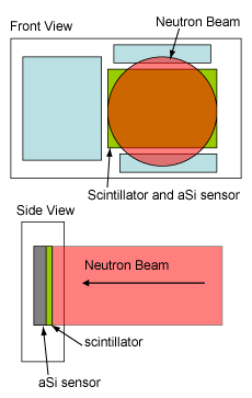
To capture the image of the light created by the scintillator there are two types of imagers. The first is a charge coupled device (CCD) type camera with a normal photographic quality focusing lens. The second is an amorphous silicon detector designed for harsh radiation environments. Since most electronics devices are sensitive to radiation damage it is necessary to protect the device from the neutron beam. The CCD camera can be easily protected by mounting it outside the beam at a 90 degree angle. The camera then focuses on the light image formed on the scintillator screen via a photographic lens. Due to the distance the camera is from the screen much of the light from the scintillator is lost, which requires long exposure times for the CCD to acquire an image (several seconds). To run a much higher speeds (30 frames per second) another system is employed that allows the sensor part to be mounted directly in the neutron beam. This is an amorphous silicon detector. This type of sensor is resistant to radiation damage. The electronics used to read the sensor are not radiation hard and are therefore designed by the manufacturer to be outside of the beam.
CCD Neutron Camera
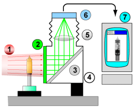
- Point source of neutrons
- Neutron to light converter
- First surface mirror (45 degree)
- Light tight box
- Standard camera lens
- Peltier cooled CCD chip
- Computer
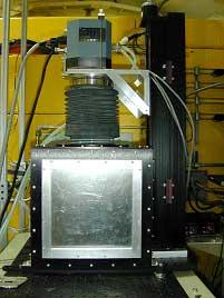
Varian Flat Panel
- Amorphous silicon
- Radiation hard
- High frame rate (30 fps)
- 127 µm spatial resolution
- No-optics - scintillator directly couples to the sensor to optimize light input efficiency
Peltier Effect
The Peltier Effect was discovered in 1834 by a French watchmaker and physicist by the name of Jean Charles Athanase Peltier (1785-1845). The Peltier Effect follows from a related effect discovered in 1821 by Thomas Johann Seebeck who showed that if heat is applied to a circuit at the junction of two different conductors a current will be generated. In 1834 Peltier demonstrated the converse effect (the Peltier effect). He found that when a current is passed through a circuit of two dissimilar conductors there will be a rise or fall in temperature at the junction depending on the direction of the current flow. One junction between the two materials becomes warm while the other cool. This electrical pumping of heat from one side of a device to the other is also known as thermoelectric cooling and is capable of cooling CCD chips to temperatures as low as -60 °C.
>>back to NIF Facility
Contacts
-
(301) 975-6465
-
(301) 975-6207
-
(301) 975-4842