U.S. flag

An official website of the United States government

Official websites use .gov
A .gov website belongs to an official government organization in the United States.

Secure .gov websites use HTTPS
A lock ( ) or https:// means you’ve safely connected to the .gov website. Share sensitive information only on official, secure websites.

Advanced Electronics Group

The Group seeks to develop the critical metrologies that will be needed in the future to understand the fundamental physics and enable advanced manufacturing of nanoscale devices at the 3 nm node and beyond.

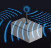
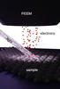
We develop new modes of spectrographic imaging or spatial resolved measurements using electrons, photons, electric or magnetic fields, or proximal probes down to the atomic scale in ambient, operating and in vivo environments. We apply Nanoscale Imaging to characterize nanoscale devices and nanostructured materials to study their physics, structure and function.

News and Updates

Projects and Programs

Advancing PEEM-based Metrology

Ongoing
Specialized imaging methods with high spatial resolution are essential for advancing the physical understanding of emergent materials in advanced electronics

Electrical Scanning Probe Microscopy

Ongoing
Develop and apply advanced measurement methods, electric field reference materials, and COMSOL models to make electrical scanning probe microscopes (eSPMs)

Publications

Awards

Press Coverage

Research Bits: Dec. 13

Semiconductor Engineering
Engineers at Caltech and the University of Southampton integrated an electronic and photonic chip for high-speed communication in data centers.

Contacts

Group Leader

General Information