
Official websites use .gov
A .gov website belongs to an official government organization in the United States.
Secure .gov websites use HTTPS
A lock (
) or https:// means you’ve safely connected to the .gov website. Share sensitive information only on official, secure websites.
NanoFab Tool: Unaxis Shuttleline DSEII Deep Silicon Etcher
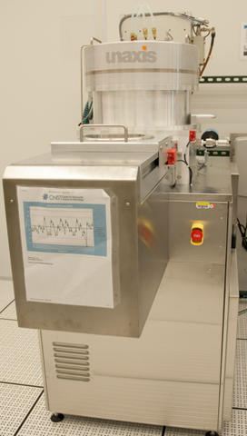
The Unaxis Shuttleline DSEII deep silicon etcher is an inductively coupled plasma (ICP) etching system used for etching deep features in silicon. The tool uses a fast switching Bosch process that produces smooth sidewall profiles while etching silicon up to 15 µm per minute. The manual load system can accommodate substrates ranging from 150 mm diameter wafers down to small pieces.
Specifications/Capabilities
- Silicon etch rate: up to 15 µm / min.
- Etch selectivity:
- Silicon to silicon oxide = 100 to 1.
- Silicon to photoresist: = 40 to 1.
- Inductively coupled plasma (ICP) power source: up to 2500 W at 2.4 MHz.
- Radio Frequency (RF) power source: up to 300 W at 13.56 MHz.
- Process Gases: Ar, O2,C4F8 and SF6
Usage Information
Supported Sample Sizes
- Maximum wafer diameter: 150 mm (6 in).
- Wafer diameters: 75 mm (3 in), 100 mm (4 in), 150 mm (6 in).
- Small pieces supported: Yes.
Typical Applications
- Microelectromechanical systems (MEMS).
- Nanoelectromechanical systems (NEMS).
- Through silicon vias (TSV) for three dimensional integration.
- Microfluidic devices.