
Official websites use .gov
A .gov website belongs to an official government organization in the United States.
Secure .gov websites use HTTPS
A lock (
) or https:// means you’ve safely connected to the .gov website. Share sensitive information only on official, secure websites.
Electronic Nanodevices Laboratory
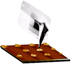
We are developing measurement and fabrication capabilities for nanoscale characterization of electronic nanodevices relevant to energy transport, storage, and conversion, and to future electronics. Next generation photovoltaic devices will be based on multi-component films formed by self-assembly or directed-assembly of donor/acceptor materials, where the essential physical and chemical processes such as charge and energy transfer occur at nanometer length scales. Similarly, as traditional complementary metal-oxide-semiconductor (CMOS) circuitry reaches the physical limits of scaling, new materials are being broadly screened for their potential integration into electronic nanodevices to extend scaling and to enable new applications beyond computation. Many potentially important materials — such as thin organic and some inorganic layers, or nanoscale objects such as chemically synthesized quantum dots and biopolymers — are either completely incompatible with conventional patterning techniques or the patterning process can significantly alter the final electronic properties of the devices. To address these problems, we are developing fabrication approaches that combine traditional and novel nanopatterning methods, and instrumentation based on advanced scanning probes with integrated detection circuitry, and thereby enable nanoscale measurement of electrical transport processes in such systems.
Location: Bldg. 216, Rm. D120
Contacts
-
(301) 975-6039