
Official websites use .gov
A .gov website belongs to an official government organization in the United States.
Secure .gov websites use HTTPS
A lock (
) or https:// means you’ve safely connected to the .gov website. Share sensitive information only on official, secure websites.
Summary
GaN nanowires grown by catalyst-free molecular beam epitaxy have the unique property that most nanowires are completely free of crystalline defects. This perfection is a direct consequence of the growth method, which approaches conditions of thermodynamic equilibrium and results in smooth sidewalls comprised of m-plane crystal planes. Our research in this area includes development of selective epitaxy methods for control of nanowire location and diameter, polarity measurement and control, doping for both p-type and n-type conductivity, and formation of quantum wells and quantum disks within the nanowires.
Description
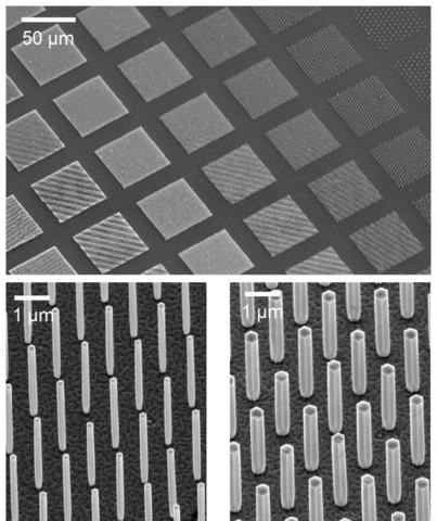
Electron microscopy images of GaN nanowire arrays at low magnification and close-ups of arrays with two different nanowire diameters.
Selective epitaxy: We have demonstrated that the diameter and placement of nanowires can be controlled by using silicon nitride (SiNx) masks on top of MBE-grown buffer layers (see figure). With electron beam lithography, several patterns with 3 mm die size that provide over 100,000 controlled nucleation sites can be generated in a few hours. The ability to control diameter is important for practical applications of GaN nanowires in manufacturing environments and is one of the key advantages they offer over other nanowire and nanotube materials. Controlling polarity of the GaN layers under the selective epitaxy mask is critical to uniform nanowire growth, as is avoiding contamination at the regrowth interface. Our selective epitaxy processes and a limited set of applications are described in U. S. Patent 9,460,21.
Polarity: Unlike many compound semiconductors, GaN forms with the wurtzite crystal structure and therefore has an axis of distinct symmetry, conventionally called the c-axis, which is aligned with the growth direction of our nanowires. The polarity of the crystal- whether the lower atom in c-plane bonds presents a Ga face or N face- determines direction of polarization fields in the crystal and also affects growth and etching rates. Reliable measurements of nanowire polarity are difficult, however, because the nanowire morphology presents different planes for etching and alters electron diffraction patterns from those established for planar films due to the 3D geometry of the nanowires. We have developed piezoforce microscopy and direct atomic imaging as methods for measuring polarity of nanowires and thin films and are researching its role in nanowire growth. These studies have shown that reactions between aluminum in the buffer layer and the silicon substrate can alter polarity during growth.
GaN nanostructure arrays with calibrated reference dimensions are available as Standard Reference Instrument 6012.