Official websites use .gov
A .gov website belongs to an official government organization in the United States.
Secure .gov websites use HTTPS
A lock (
) or https:// means you’ve safely connected to the .gov website. Share sensitive information only on official, secure websites.
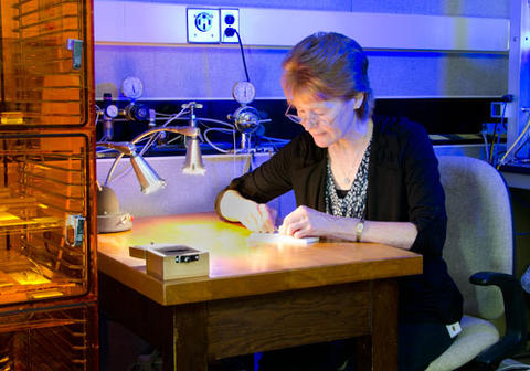
PML researcher Janet Cassard examines samples of the two new Reference Materials to be used for calibrating microscale measurements on MEMS devices.
Over the past two decades, microelectromechanical systems (MEMS) have become ubiquitous, with applications in cell phones, ink-jet printers, accelerometers and inertial sensors, tiny transducers and actuators, and scores of other devices. Increasing numbers of applications in the near future are anticipated in the health care arena with, for example, point of care testing.
What has not been ubiquitous – until now, with the release of NIST's first MEMS reference materials – is an authoritative set of mathematical and physical standards for testing the properties and performance of MEMS components. As a result, manufacturers and designers have lacked a way to validate in-house measurements for consistency to reconcile measurement differences between suppliers and customers.
"The problem," says Janet Cassard of PML's Semiconductor and Dimensional Metrology Division, "is that there are many different ways to measure, say, a parameter such as Young's modulus. That was a big problem in the community because people were using different structures and techniques and their results would be off by a factor of two. There was no consensus about proper test structures or test methods."
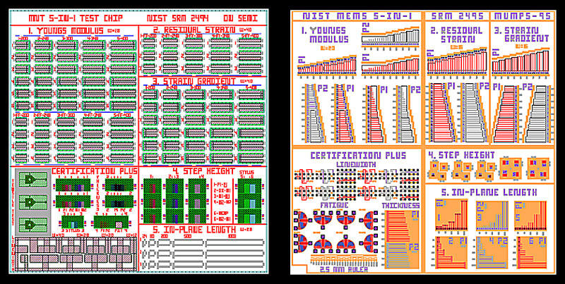
Cassard and colleagues began addressing those problems more than a decade ago. In 2001 they produced the beginnings of an online MEMS calculator that has evolved into Standard Reference Database 166, which computes reference values for each of eight properties - Young's modulus, residual stress, stress gradient, residual strain, strain gradient, step height, thickness, and in-plane length – tailored to individual circumstances.
Users enter data for dozens of variables relevant to the parameter of interest. Then the program, written by Cassard and employing ASTM and SEMI standards, performs the calculations. If the software identifies a problem in one or more fields, the output displays a "wait" warning alerting the user to check the data. "The database ensures that everybody is doing the calculations in exactly the same way," Cassard says.
The new reference materials (RM 8096 and 8097), for expected release in 2013, are two different versions of "5-in-1" test chips containing reference microstructures to be used in five test methods: Young's modulus, residual strain, strain gradient, step height, and in-plane length. (Actually, by using the calculations or measurement techniques provided in the Young's modulus and step height test methods, users can obtain eight properties: the five listed above plus residual stress, stress gradient, and beam thickness.)
Using the chips, companies can take local measurements of features on the RMs and compare their measurements with those of NIST on exactly the same features to evaluate their use of the test methods. The skill set obtained from the proper use of the RMs enables companies to validate and troubleshoot a process. In addition, the chips can be used to calibrate an instrument. However, they are not optimized for calibration, so the uncertainties are much larger than those for artifacts specifically intended for this purpose.
RM 8096 is fabricated using a standard CMOS process for which the electrical performance is optimized. The topography is etched at NIST using bulk-micromachining. Properties of the composite oxide layer are reported. Each unit measures about 5 mm square.
RM 8097, approximately 1 cm square, is optimized for mechanical MEMS structures. It is fabricated with a semi-custom polysilicon process with a backside etch; properties of its first or second polysilicon layer are reported.
The 5-in-1 RMs are intended for use by MEMS designers, IC and MEMS foundries and services, and equipment manufacturers (including manufacturers of film deposition systems). The instruments used for the RM measurements include optical vibrometers, optical interferometric microscopes, and stylus profilometers (or comparable instruments).
Cassard first presented the chips at the SEMICON WEST meeting on July 10, 2012. "It's time to interact with instrument manufacturers who would like to capture the MEMS market by offering immediate test method calculations on their instruments. This can be done via the incorporation, within their software, of the pertinent MEMS Calculator data sheets, with added input and output capability," says Cassard. "This is currently being considered by at least one company."
The RMs are expected to be offered for sale in 2013 in limited quantities, with RM 8096s priced at approximately $2,000 each, and RM 8097s at approximately $1,500. Each customer will also receive: a hardcopy of the five standard test methods; an electronic version of the User's Guide; a hard and soft copy of the pertinent MEMS calculator web pages with NIST's data for the purchased RM as the sample data; and an RM Report of Investigation which provides the NIST reference values obtained from the data sheets.
Another batch of 41 RMs is now being tested. Depending on demand, more may be fabricated. If the devices prove to have a large audience, NIST plans to turn over production to a suitable firm or firms.
"Getting the equipment manufacturers on board, that's the next thing, then passing the whole nine yards to a standards company," says Jon Geist, Project Leader for the 5-in-1. "[The RM process] will be a success if we can hand it off to a company to carry on."
The designation "reference material" means that NIST has determined that an object's property values are sufficiently homogenous, stable, and well established so that they can be used, for example, for the assessment of a measurement method. This makes the material suitable for further research and for determining the efficacy of a prototype.
It is not yet clear whether the MEMS community will want or can benefit from the highest level of NIST certification – a Standard Reference Material, which NIST has certified and released specifically to be used to develop accurate methods of analysis, to calibrate measurement systems, and to ensure adequacy and integrity of measurement assurance programs.
"It is an exciting time for the MEMS community, as it is poised to become an integral part of the $1.3 trillion electronics industry which has had such a tremendous impact on our society," says David Seiler, Chief of the Semiconductor and Dimensional Metrology Division. "NIST has been a leader in the MEMS field since the early 1990s when it helped stimulate CMOS MEMS fabrication methods into commercial CMOS foundries. The NIST reference materials will provide the foundation for innovations in fields like mobile and medical electronics."
-- written by Delilah Gates