Official websites use .gov
A .gov website belongs to an official government organization in the United States.
Secure .gov websites use HTTPS
A lock (
) or https:// means you’ve safely connected to the .gov website. Share sensitive information only on official, secure websites.
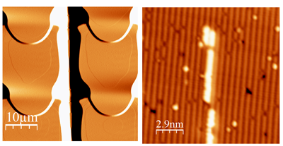
Left: Large atomic terraces. Right: Atomic resolution patterning by scanning tunneling microscope.
As features on silicon microchips continue to shrink, the final frontier of miniaturization is a transistor on the scale of a single atom – a technology that could revolutionize computing.
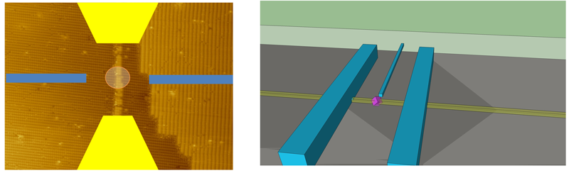
PML has begun a new research program to create just such a device in manufacturable, solid-state form by harnessing two capabilities unique to NIST.
One is the ability to precisely place individual dopant atoms on a silicon surface and create atomically aligned etch masks using a technique called hydrogen-based scanning probe lithography. Detecting and manipulating the states of those atoms, however, would be nearly impossible unless they are placed in a perfectly uniform lattice – a condition made possible by an unmatched NIST capability to make the world's most highly enriched silicon-28, most recently at 99.9999% purity.
When fully developed and characterized, the devices would not only yield unprecedented insights into conventional semiconductor performance, but would define a viable path to manufacturable atom-based solid-state quantum computing and the ultimate limit for scaling electronic devices.