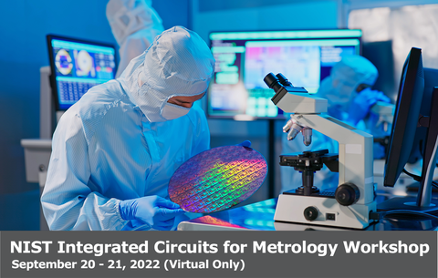
Metrology for electronics and computing systems has historically revolved around bench top test systems and wafer level probing of parametric test structures for building models of devices. However, as the ecosystem for designing integrated systems has matured, more complex systems for measurement and self-test have emerged, such as array level testing macros for transistors and memory devices, the use of embedded high frequency oscillators and sources for AC measurement, and the fabrication of even embedded sensors for magnetic fields or temperature. Such test vehicles can dramatically improve the sensitivity, bandwidth, and scale of measurements and compensate for parasitic losses in traditional cabling and provide local, real-time insight into the more complex physical properties of a test structure. Hardware systems for Artificial Intelligence, especially those based on neuromorphic or analog elements, critically require scaled measurements to connect the performance of individual memory elements or neurons to the system level performance. For other sophisticated prototypes in research and development, such as biological, superconducting, or photonic systems heterogeneously or monolithically integrated with foundry semiconductors, test vehicles are essential for predicting the performance of the final, functioning system.
Working Group Meeting on the Nanotechnology Accelerator Platform
Day 2 includes a working group meeting to discuss the development of non-proprietary, open-source designs for metrology of monolithically integrated electronic devices with CMOS. Contributions are needed from circuit designers, device engineers, nanofabrication engineers, and scientists to develop designs and methodologies for the use of parametric test structures and reference prototypes for a diversity of applications including but not limited, 2 or 3 terminal memory devices, thin film transistors, 2D materials, bioelectronics, superconducting-semiconducting integration, plasmonics, radiofrequency electronics, and artificial intelligence. These designs will ultimately be manufactured and made available in the SKY130 process node. This meeting will include an introductory presentation followed by open discussion
workshop objectives
The first goal of this workshop is to discuss parametric test structures and system prototypes on an increasing scale – from monolithically integrated to packaged into a small die – and the role of the semiconductor foundry supply chain for enabling research into this area using integrated circuit designs and chips for metrology. The second goal of this workshop is to convene a working group meeting of researchers, scientists, and engineers to work towards the creation of a non-proprietary open-source set of test vehicles for monolithic integration in the back-end-of-line with CMOS. These designs would be freely available to use and reference, but, through an additional public-private partnership, will also become available in a wafer-scale formfactor to be directly sourced from a U.S. domestic semiconductor foundry as a testbed for semiconductor manufacturing R&D.
Agenda & speaker bios
View/Download Agenda HERE

