
Official websites use .gov
A .gov website belongs to an official government organization in the United States.
Secure .gov websites use HTTPS
A lock (
) or https:// means you’ve safely connected to the .gov website. Share sensitive information only on official, secure websites.
Summary
|
Our goal is to provide industry with test structures and models of next-generation photovoltaics, with an initial focus on cadmium telluride (CdTe) and CuInxGa1-xSe2 (CIS or CIGS) materials. These |
tools will enable interpretation of measured external properties affected by three-dimension (3D) geometry, grain structure, and nanoscale phase separation, supporting improved processing and design of Second Generation (thin film) and Third Generation (nanostructured) photovoltaic devices.
Description
First Generation (thick layers of crystalline silicon) and Second Generation (thin films of CdTe, CIGS, and related materials) PV devices are both well established in the marketplace, with well defined techniques for fabrication and characterization. Third Generation PV encompasses a wide diversity of materials and nanostructures and commercially viable technologies and means of fabrication are yet to be determined. Many of of the proposed structures have considerable microstructural variability that complicate interpretation of macroscopic device measures. The aim of this project is to develop idealized, three-dimensionally patterned templates that can serve as test structures to enable measurement of critical device and materials properties.
One of the most attractive properties of CdTe and CIGS for photovoltaic applications is their amenability to a variety of cost-effective fabrication methods, including sputtering, printing, and electrodeposition. We are developing three-dimensionally patterned photovoltaic test structures as well as fabrication processes including electrochemical deposition to enable the impact of geometry and internal defect structures on efficiency and broader photoelectrical properties to be determined.
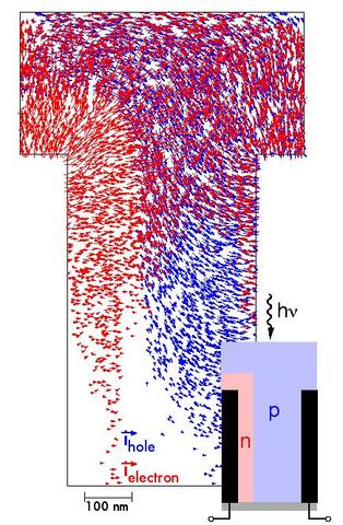
To guide and interpret the experimental measurements we are developing models of light and charge transport within arbitrary 2D and 3D semiconductor and device geometries. These models will ultimately include the full effects of optical re-fraction and reflection that are relevant to all PV devices but play a particularly important role in 3D structures.
Major Accomplishments
|
In FY10 we substantially expanded our nascent effort to develop photovoltaics templates with 3D microstructures for application to 3rd Generation Photovoltaics through joint funding with NIST's CNST and EEEL from the NIST Director's Innovation in Measurement Science program. A focus of this major new effort remains developing structures with adjustable, well-defined geometries that are applicable to a broad set of materials and consistent with insightful measurements and interpretation of the properties of 3D photovoltaics. |
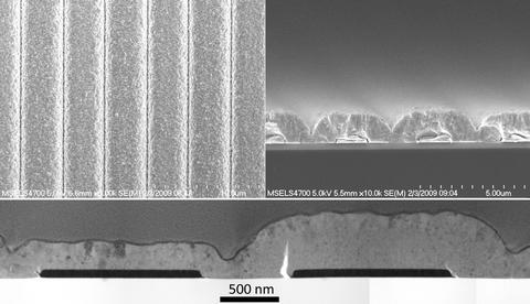
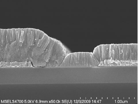
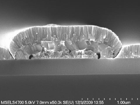
| In collaboration with the CNST we have developed the capability to fabricate photovoltaic test structures using a set of interdigitated back-contact electrodes. These electrodes are used to independently electrodeposit one or more of the p- and n-type semiconductors that constitute the active device. After deposition, the same contacts are also used to extract light-generated current from the device as well as for electrical characterization. |
|
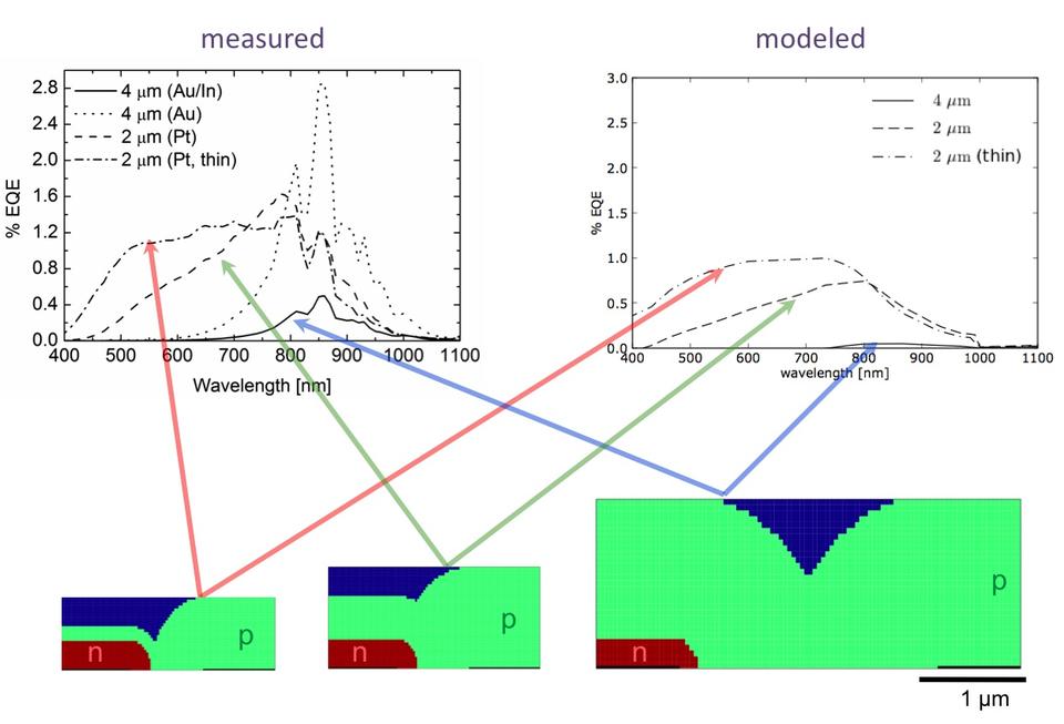
Using an early-generation model, we were able to create simulations of the external quantum efficiency (EQE) that successfully captured major trends in the measured performance of CdTe devices over a range of illuminating wavelengths for three different device geometries.
- Josell D, Beauchamp CR, Jung S, Hamadani BH, Motayed A, Richter LJ, Williams M, Bonevich JE, Shapiro A, Zhitenev N, Moffat TP, "Three Dimensionally Structured CdTe Thin-Film Photovoltaic Devices with Self-Aligned Back-Contacts: Electrode-position on Interdigitated Electrodes," Journal of the Electrochemical Society 156:H654 (2009)
- Josell D, Beauchamp CR, Hamadani BH, Jung S, Guyer JE, Hangarter C, Motayed A, Hangarter C, Gergel-Hackett N, Xu H, Zhitenev N, "Three-Dimensionally Structured Thin Film Heterojunction Photovoltaics on Interdigitated Back-Contacts," ECS Transactions 28:521 (2010)
Additional Technical Details
Initial studies focused on devices composed solely of CdTe. By independently adjusting the potential of each set of electrodes, different stoichiometries were obtained, allowing the deposition of p- and n-type material from the same electrochemical bath on the two different electrodes. These structures demonstrated the proof of concept for more typical devices based on two different semiconducting materials (heterojunctions). Electrical, optical, and structural characterization was performed, in concert with the CNST and CSTL.
More recently we extended the study of these structures to include heterojunctions, which should lead to both better device performance and will significantly expand the range of industrially relevant materials and combinations that we can study. Thus far, we have combined our extant CdTe electrodeposition capability with sputtered indium-tin-oxide (ITO), electrodeposited CdS, and sol-gel deposited titanium oxide.
To support this experimental effort, we have developed a photovoltaic device model that gives us complete control over geometry and microstructure. We implemented our device model in the FiPy partial differential equation solver package. This freely available pack-age, developed within the Metallurgy Division, allows us to easily distribute our photovoltaic codes to researchers in industry and elsewhere as they are validated. Because it was designed to model phase transformations, FiPy will also allow us to examine the effect of microstructures obtained from rigorous thermodynamic and kinetic modeling.
Associated Product(s)
We implemented our device model in the FiPy partial differential equation solver package, http://www.ctcms.nist.gov/fipy, developed in the Metallurgy Division. This freely available package allows us to easily distribute our photovoltaic codes to researchers in industry and elsewhere as they are validated.
Project Summary (PDF)