
Official websites use .gov
A .gov website belongs to an official government organization in the United States.
Secure .gov websites use HTTPS
A lock (
) or https:// means you’ve safely connected to the .gov website. Share sensitive information only on official, secure websites.
Summary
In this project, we are developing metrology needed for the synthesis, processing, and characterization of semiconductor nanowire structures to enable reliable nanoscale device development for electronic, photonic, and sensor applications. The project focuses on the measurement of structural and electronic properties enabling performance measurements of nano-devices, and determining and disseminating key data related to nanowire processing, structure, properties, and device performance.
Description
One of the key issues hampering progress in semiconductor nanotechnology is the absence of standardized nanostructures. We address this need through the controlled fabrication and assembly of semiconductor nanowire test structures with well-defined properties. To achieve this, we have manufactured two custom-designed versatile chemical vapor deposition (CVD) reactors for group III nitrides and for silicon growth, respectively. Using these tools in combination with catalyst-facilitated vapor-liquid-solid (VLS) growth concepts, post-growth assembly techniques, and comprehensive structural/electrical/optical measurement capabilities will enable new approaches for making GaN- and Si- based advanced nano test structures with desired properties. As we progress, we plan to extend these approaches to new classes of semiconductor materials as guided by emerging nanotechnology needs of our customers. These unique standardized test structures can ultimately be used for photonic, electronic, nano-electromechanical, and sensor applications

Major Accomplishments
- The fabrication and comprehensive characterization of semiconductor nanowire test structures at NIST is intended to enable development and commercialization of novel NW-based materials and device structures for photonic, electronic, nano-electromechanical, and chemical/bio-sensor applications.
- Industrial Customers include: Applied Materials (GaN-based thin film and nanowire structures); GeneSiC Semiconductors (SiC nanowires); Blue-wave Semiconductors (UV-detectors and sensors based on ZnO nanowires).
- Government agencies following this work include DARPA, DOE, and DTRA.
"The work of NIST team on GaN nanowire-based LEDs bridges the gap between current micro-technology and new nanoscopic elements in a very elegant way. Technologically speaking, this is a real-to-go nanowire device."
-- Nanomaterials News, v. 3 , Issue 8, 26 June 2007; IntertechPira.com
As the microelectronics industry moves toward new-generation nano-devices, materials challenges persist in fabricating nanostructures with desired properties. These challenges are due to the inability to control morphology and structural quality of nanostructures, the inherent material thermal instability, uncontrolled phase separation, etc. The ability to measure these parameters is necessary in order to understand the processes for reliable design for fabricating and evaluating nanostructured devices.

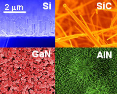
In-house capabilities for fabrication, processing, and structural, electrical, and optical measurements of semiconductor nanowire test structures have been jointly developed at both Metallurgy Division (MML) and Optoelectronics Division (PML-Boulder) sites. The design and installation of two chemical vapor deposition (CVD) reactors for Group III nitrides and for silicon nanowire & thin-film growth have been completed at MML. The growth systems became an essential part of the existing and future nano-science / technology programs of the Metallurgy Division. Initial experiments have demonstrated successful fabrication of GaN nanowires, AlN nanocones, and Si nanowires on various substrates (see insert at the top of a previous page). NIST has worked with industrial and academic partners to develop SiC, InN, ZnO, and Te nanowires. A measurement platform for electrical (4-probe system equipped with an environmental chamber with controlled atmosphere, temperature, and magnetic field; see figure on the previous page) and optical (UV-visible detector with micro-waveguides) characterization of nanowires has been developed.
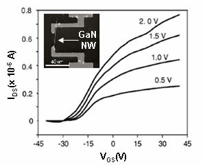
This comprehensive set of fabrication and measurement tools enabled the demonstration and evaluation of two key nanowire device structures: GaN NW based field-effect-transistor (NWFET) and novel light-emitting diode (LED). The figure to the top right shows an actual NWFET and its electrical characteristics. Highest electron mobilities of 319 cm2/V⋅s, current "on/of" ratio of 107 and normalized transconductance of 325 µS/mm were achieved on a 200 nm diameter GaN NWFET. Comprehensive characterization of the NWFET set revealed the dependence of device transport properties on the NW diameter and structural perfection. This study has demonstrated the importance of correlating the "processing-structure-property-performance" relation-ship and of controlled fabrication of NWs with defined structural and electronic properties.

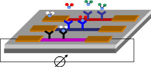
The NW LED, shown in the figure to the bottom right, is a first demonstration of GaN homo-junction n-nanowire/p-substrate electro-lumincescent device. A set of nano-LEDs with 365 nm emission wavelength was fabricated using NW dielectrophoretic alignment and CMOS-compatible batch fabrication processes. The simplicity, reproducibility, and scalability of the approach could enable industrial manufacturing of nano-LEDs and nano-lasers for photonic and sensor applications.
Project Summary (PDF)