
Official websites use .gov
A .gov website belongs to an official government organization in the United States.
Secure .gov websites use HTTPS
A lock (
) or https:// means you’ve safely connected to the .gov website. Share sensitive information only on official, secure websites.
Summary
This project is developing means of quantitatively measuring chemical distributions in three dimensions at the nanometer scale in materials with complex heterogeneities. The 3D chemical imaging and reconstruction methods being developed will compete with and add value to current 3D morphologic analysis techniques. With these developments, we hope to promote the application of electron microscopy methods to the advanced characterization of materials structure, morphology and composition at the nanometer scale.
Description

Due to projection effects, analytical transmission electron microscopy (AEM) of thinned or sectioned samples has traditionally been limited to essentially two-dimensional imaging and analysis. Current nanometer scale devices are too small and complex for current sectioning capabilities and two-dimensional analysis since the electron beams pass through more than one device component. Moreover, existing approaches to acquire spectral images are too time-consuming and impractical. For example, a one second collection time taken at each nanometer-sized pixel of a 1,000 by 1,000 pixel image requires about 12 days.
Our approach produces 3D elemental maps using chemical tomography, based on tilt series of spectroscopic data in the AEM. The practicality of this approach has been demonstrated recently by the successful generation of experimental 3D elemental maps from nanometer-scale sample data acquired in the laboratory. Significant challenges of diffraction contrast and automating the AEM acquisition of spectral datasets have been addressed by a NIST team of scientists from MML, PML, and ITL.
Major Accomplishments
- Broadly useful measurement approaches being developed will for the first time yield 3D chemical information of real nanotechnology devices, enabling higher throughput/higher speed chemical nanoscale mapping, intelligent imaging and analysis, and determination of effects due to structure, chemical spectroscopies, and morphology.
- NIST has worked extensively with microscope manufacturers such as FEI Company as well as instrumentation vendors (Fischione, Gatan, 4pi) on design and refinement of their spectroscopy and tomography systems.
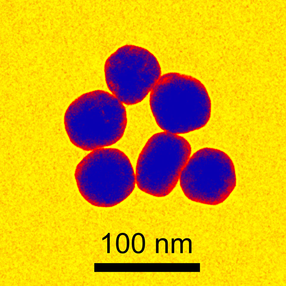
- NIST partnered with the National Cancer Institute's Nanotechnology Characterization Laboratory (NCI/NCL) to develop and characterize nanoscale gold particles in the 10 nm, 30 nm, and 60 nm size regimes.
- Electron microscopy methods have been used to characterize potential reference materials such as single-walled carbon nanotubes and strain-free diffraction calibration materials.
Nanometer-scale compositional 3D measurement tools are in their infancy and must overcome critical measurement barriers to be practical. Only a few laboratories can attempt these types of experiments, and NIST is providing leadership in developing the necessary metrology infrastructure.
In 3D analysis, the third dimension must be deconvolved from a series of 2D projections to understand the chemical construction of a device. However, diffraction contrast in crystalline materials challenges the underlying tomography assumptions and has been addressed by employing large angle convergence scanned beam illumination (LACSBI), a new electron optical technique.
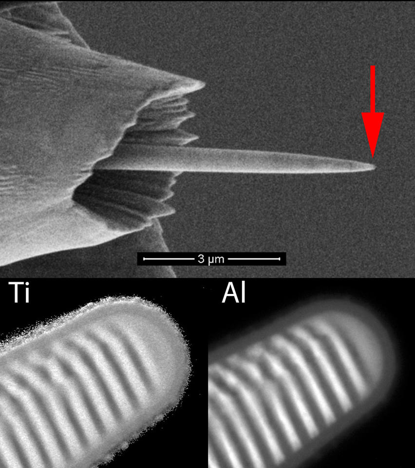
Automating the AEM acquisition of hyper-spectral datasets (combining imaging with X-ray energy dispersive and electron energy loss spectroscopies) has required a new generation of instrumentation. MML teamed with FEI Company to acquire a new 300 kV aberration-corrected TEM with advanced computer controls. In addition, conventional tomography holders can not eliminate a "missing wedge" of data. MML worked with Fischione Instruments to devise a new holder that accepts cylindrically symmetric samples with full 360 degree rotation freedom. Focused ion beam (FIB) tools and automated routines are used to prepare suitable probe-shaped samples. Such samples are also amenable to analysis in atom probe instruments.
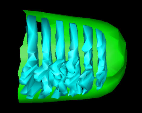
We have combined these developments (new AEM, LACSBI, FIB and holders) to reconstruct 3D chemical data in industrially relevant materials, see figure below. Here, a multilayer film of Ti and Al (with 20 nm bilayer repeats) was deposited by electron-beam evaporation. A section of this film was then FIB-extracted, placed onto the tomography holder stub and FIB'd into a electron transparent probe tip. Using LACSBI to suppress diffraction effects, the two-element chemical data was acquired over 360° at 2° increments. The resulting data were reconstructed with better than 5 nm resolution to create a 3D model of the sample that clearly revealed the grain boundary in the film (see figure below).
NIST partnered with the NCI/NCL in a program led by the Ceramics Division to develop and characterize nanometer-scale gold particles in the 10 nm, 30 nm and 60 nm size regime (RM8011, RM8012, and RM8013). TEM was used as the most direct method to measure particle diameter, via the projected image of particles deposited onto an electron-transparent substrate. The internal structure and surface morphology were characterized and compared with measurements made by SEM and AFM. Special procedures were used to minimize agglomeration and over 12,000 particles were analyzed using custom software. Particle size was determined by the "equivalent diameter" approach to minimize the effects of surface faceting. Likewise, particle agglomerates were excluded from the size analysis. This program resulted in the first commercially available nano scale reference materials.
Project Summary (PDF)