
Official websites use .gov
A .gov website belongs to an official government organization in the United States.
Secure .gov websites use HTTPS
A lock (
) or https:// means you’ve safely connected to the .gov website. Share sensitive information only on official, secure websites.
Summary
Measuring interactions between light and matter has both fundamental and practical importance. For example, lasers have had a profound influence on science and industry over the past 50 years. More recently, devices exploiting light-matter interactions at the smallest scale, between a single photon and a single atom, have been a proving ground for ideas in quantum mechanics and a test bed for quantum-information-processing applications. Our goal is to develop measurement tools to probe these interactions in solid-state systems. We focus on nanoscale materials such as epitaxially grown quantum dots and solution-processed colloidal nanocrystals, and perform measurements on these nanostructures both "as-grown" and also when integrated into nanofabricated devices like optical cavities.
Description
A "single emitter" is a structure that exhibits a transition from a high energy state to a low energy state, thereby generating a photon, or light emission. A variety of solid-state single emitters have been discovered or manufactured. One example is a quantum dot, a nanometer-scale structure that is sometimes called an "artificial atom" because it exhibits many properties of a single atom, even though it actually consists of thousands of atoms. Various technologies have been developed to isolate individual atoms, molecules, ions, and other single emitters, and to study their optical properties. For example, light in an optical cavity can be localized to a small volume and persist for thousands of cycles before decaying, providing the dual benefit of a strong electromagnetic field and a long interaction time. This forms the basis of cavity-enhanced optical spectroscopy, one important aspect of this project.
This project involves measurements on two solid-state cavity-quantum dot systems operating at technologically important telecommunications wavelengths. The first measures interactions between a single epitaxially-grown InAs quantum dot and a GaAs optical cavity. The second measures the interactions of an ensemble of solution-processed PbS nanocrystal quantum dots with a Si optical cavity. Prospective applications of these systems might include low-power optical switching, a host of light-emitting devices, including those that produce single photon pulses for cryptography, and new components for quantum information processing networks.
Performing measurements on such small systems is one of the principal challenges of this work. We accomplish this with an optical fiber taper waveguide, fabricated out of standard telecommunications optical fiber. The waveguide diameter starts at 125 micrometers, standard for an optical fiber, and gradually decreases to about 1 micrometer, before gradually increasing back to 125 micrometers. The tapered fiber is positioned so that its narrowest section is adjacent to the cavity (Figs. 1b and 2b.) At this juncture, a fraction of the light sent through the waveguide then tunnels into the cavity, where it interacts with the quantum dot(s). Some of the light in the cavity then tunnels back into the waveguide, and we measure the properties of this exiting light to identify signatures of the quantum dot interaction.
Cavity quantum electrodynamics with a single InAs quantum dot
This project is in collaboration with colleagues at the California Institute of Technology and the University of Rochester. The cavity geometry we have focused on is the microdisk, consisting of a small GaAs disk on top of an AlGaAs pedestal (Fig. 1a). The microdisk supports "whispering gallery modes", in which light circulates around the periphery of the structure thousands of times before dissipating. Housed within the microdisk cavity is an InAs quantum dot, a small island of InAs that is several nanometers in diameter and a few nanometers in height. To minimize unwanted decay processes in the quantum dot, the chip is cooled to below 15 Kelvin in a customized cryogenic fiber probe system.
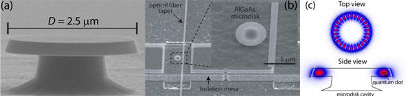
Fig. 1. (a)-(b) Scanning electron microscope images of a chip-scale microdisk-quantum dot system, accessed by a fiber taper waveguide. (c) Optical field within a microdisk cavity, with the preferred quantum dot position schematically indicated.
If the cavity is small enough and the rate of light loss and quantum dot decay is low, the interaction between a single photon in the cavity and the quantum dot can be stronger than any decay process in the system. In this "strong coupling" regime of cavity quantum electrodynamics, the quantum dot and the light wave form a coupled quantum system, similar to two atoms forming a molecule. Reaching this strong coupling regime in which quantum mechanical interactions dominate is a prerequisite for many important applications in future generations of information processing.
Measurements performed thus far include spectroscopy to confirm that a strongly-coupled system has been formed, and studies of its linear and nonlinear properties. One exciting result with implications for switching applications has been the demonstration of nonlinear behavior for ultra-low input powers. As our experiments progress, we hope to increase the efficiency, sensitivity, and stability of our measurements through improvements in the cavity/fiber waveguide system and in our cryogenic probe station.
Silicon nanophotonics with PbS quantum dots
Though the above work focuses on InAs quantum dots in GaAs nanophotonic structures, the architecture of a single emitter interacting with a strongly confined optical field and read out by the fiber taper waveguide is general, and can be applied to numerous systems. In collaboration with colleagues at Columbia University, we are characterizing silicon cavities integrated with lead sulfide (PbS) colloidal quantum dots. Although silicon is the basic building material for modern information technology, light emission from silicon is intrinsically difficult. The integration of silicon devices with PbS quantum dots which emit in the 1.55 µm telecommunications band may lead to important devices for classical and quantum information processing. A particular measurement challenge for this system is the low emission level produced by the PbS quantum dots, which limits the degree to which the system can be effectively characterized, particularly when the quantum dot density is reduced. As a result, the advantageous properties of the fiber taper waveguide measurement approach may be particularly important within this system.
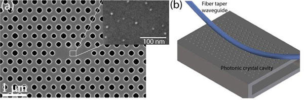
Fig. 2. (a) Scanning electron microscope image of a silicon photonic crystal cavity containing PbS quantum dots (b) Schematic of the fiber coupling approach.
We have recently used the fiber taper method to interrogate a low density of PbS quantum dots that have been spun onto silicon photonic crystal cavities (Fig. 2). We have confirmed that the quantum dot integration does not degrade the cavity's loss, and have performed measurements of cavity-filtered photoluminescence, looking at effects such as quantum dot "blinking" (fluorescence intermittency) and saturation. Going forward, we hope to improve the sensitivity of measurements on this system, eventually achieving the capability to characterize a single PbS quantum dot.
Selected Publications
- Bright single-photon emission from a quantum dot in a circular Bragg grating microcavity, S. Ates, L. Sapienza, M. Davanco, A. Badolato, and K. Srinivasan, IEEE Journal of Selected Topics in Quantum Electronics 18, 1711 –1721 (2012).
NIST Publication Database Journal Web Site - Telecommunications-band heralded single photons from a silicon nanophotonic chip, M. Davanço, J. R. Ong, A. B. Shehata, A. Tosi, I. Agha, S. Assefa, F. Xia, W. M. J. Green, S. Mookherjea, and K. Srinivasan, Applied Physics Letters 100, 261104 (2012).
NIST Publication Database - A circular dielectric grating for vertical extraction of single quantum dot emission, M. Davanço, M. T. Rakher, D. Schuh, A. Badolato, and K. Srinivasan, Applied Physics Letters 99, 041102 (2011).
NIST Publication Database - Fiber-based cryogenic and time-resolved spectroscopy of PbS quantum dots, M. T. Rakher, R. Bose, C. W. Wong, and K. Srinivasan, Optics Express 19, 1786-1793 (2011).
NIST Publication Database Journal Web Site - Spectroscopy of 1.55 μm PbS quantum dots on Si photonic crystal cavities with a fiber taper waveguide, M. T. Rakher, R. Bose, C. W. Wong, and K. Srinivasan, Applied Physics Letters 96, 161108 (2010).
NIST Publication Database - Investigations of a coherently driven semiconductor optical cavity QED system, K. Srinivasan, C. P. Michael, R. Perahia, and O. Painter, Physical Review A 78, (2008).
NIST Publication Database Journal Web Site - Linear and Nonlinear Optical Spectroscopy of a Strongly-Coupled Microdisk-Quantum Dot System, K. Srinivasan and O. Painter, Nature 450(7171), 862-865 (2007).