
Official websites use .gov
A .gov website belongs to an official government organization in the United States.
Secure .gov websites use HTTPS
A lock (
) or https:// means you’ve safely connected to the .gov website. Share sensitive information only on official, secure websites.
NanoFab Tool: JEOL JBX 6300-FS Direct Write Electron Beam Lithography System
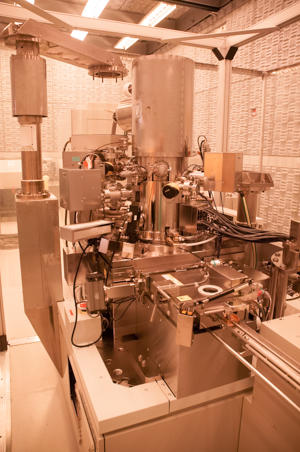
Photograph of the JEOL JBX 6300-FS Direct Write Electron Beam Lithography System.
The JEOL JBX 6300-FS direct write electron beam lithography system allows users to quickly and directly pattern a variety of substrate materials with feature sizes as small as 10 nm. The high precision stage provides excellent pattern stitching and can accommodate substrates ranging from 200 mm diameter wafers down to small pieces.
Specifications/Capabilities
- Accelerating voltage: 100 keV.
- Spot size: 2 nm.
- Scan rate: 50 MHz.
- DAC resolution: 19 bit.
- Write field: 0.5 mm (4th lens).
- Step and scan writing to pattern large areas.
- Stitching accuracy: < 20 nm.
- Overlay accuracy: < 20 nm.
Usage Information
Supported Sample Sizes
- Maximum wafer diameter: 200 mm (8 in).
- Small pieces supported: Yes.
Typical Applications
- Microphotonic and nanophotonic devices.
- High density magnetic nanopillars.
- CMOS devices.
- MEMs and NEMs structures.
- Dot arrays and lines with feature sizes < 20 nm.
Created May 2, 2014, Updated February 24, 2023