
Official websites use .gov
A .gov website belongs to an official government organization in the United States.
Secure .gov websites use HTTPS
A lock (
) or https:// means you’ve safely connected to the .gov website. Share sensitive information only on official, secure websites.
NanoFab Tool: Bruker Dektak XT Profilometer
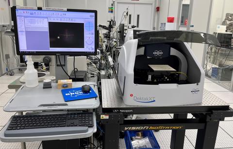
Bruker Dektak XT Profilometer
The Bruker Dektak XT contact profilometer measures the thin film thickness of patterned features by sensing the deflection of a fine stylus that is raster scanning over features ranging in height from 1 mm down to 5 nm. It is capable of mapping step heights and displaying topological three dimensional images of substrates ranging from 200 mm diameter wafers down to small pieces.
Specifications/Capabilities
- Maximum step height: 1 mm.
- Vertical resolution: 0.1 nm.
- Scan length: 50 um to 50 mm.
- 120,000 data points per scan.
- Scans can be stitched end to end to span up to 150 mm.
- Stylus force: 0.098 mN to 147 mN (0.01 mgf to 15 mgf).
- Motorized X-Y-theta stage.
- Wafer mapping up to 150 mm.
- 3-D topological imaging.
Usage Information
Supported Sample Sizes
- Maximum wafer diameter: 200 mm (8 in).
- Small pieces supported: Yes.
- Maximum thickness: 50 mm.
Typical Applications
- Measurement of etch rates, deposition rates, and film growth rates.
- Measurement of surface roughness.
- Thickness mapping.