
Official websites use .gov
A .gov website belongs to an official government organization in the United States.
Secure .gov websites use HTTPS
A lock (
) or https:// means you’ve safely connected to the .gov website. Share sensitive information only on official, secure websites.
Designer Materials Through Controlled Nanocrystal Coupling for Electronic and Optical Applications
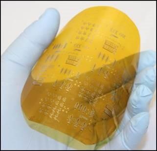
Semiconductor and plasmonic nanocrystals are known for their size- and shape-dependent photoluminescence and localized surface plasmon resonances respectively. In this talk, I will describe the use of semiconductor and plasmonic nanocrystals as building blocks of mesoscale materials for semiconductor electronics and optoelectronics and plasmonic optical metamaterials. Chemical exchange of the long ligands used in nanocrystal synthesis with more compact ligand chemistries brings neighboring nanocrystals into proximity and increases interparticle coupling. In semiconductor nanocrystal solids, we show strong electronic coupling in combination with doping allows us to control the carrier type and concentration and design high mobility n- and p-type materials. I will give examples where n- and p-type nanocrystal solids are used to construct field-effect transistors and integrated circuits and solar photovoltaics. In metal nanocrystals, ligand-controlled coupling allows us to tailor a dielectric-to-metal phase transition seen by a 1010 range in DC conductivity and a dielectric permittivity ranging from everywhere positive to everywhere negative across the whole range of optical frequencies. We realize a "diluted metal" with optical properties not found in the bulk metal analog, presenting a new axis in plasmonic materials design and the realization of optical properties akin to next-generation metamaterials. We harness the properties of metal NCs by using nanoimprint lithography to print large-area metamaterials on glass and plastics with widely tailorable optical properties that are used to realize near-infrared optical devices.
Sponsors
For further information please contact robert.ilic [at] nist.gov (Robert Ilic), 301-975-2639
Cherie R. Kagan
University of Pennsylvania, Department of Electrical and Systems Engineering, Department of Materials Science and Engineering, Department of Chemistry